INTELLECTUM VIRTUS
INTELLECTUM VIRTUS
INTELLECTUM VIRTUS
INTELLECTUM VIRTUS
INTELLECTUM VIRTUS
ELECTRICAL ENGINEERING
ELECTRICAL ENGINEERING
ELECTRICAL ENGINEERING
ELECTRICAL ENGINEERING
ELECTRICAL ENGINEERING
SEMICONDUCTOR REGISTER
SEMICONDUCTOR REGISTER
SEMICONDUCTOR REGISTER
SEMICONDUCTOR REGISTER
SEMICONDUCTOR REGISTER
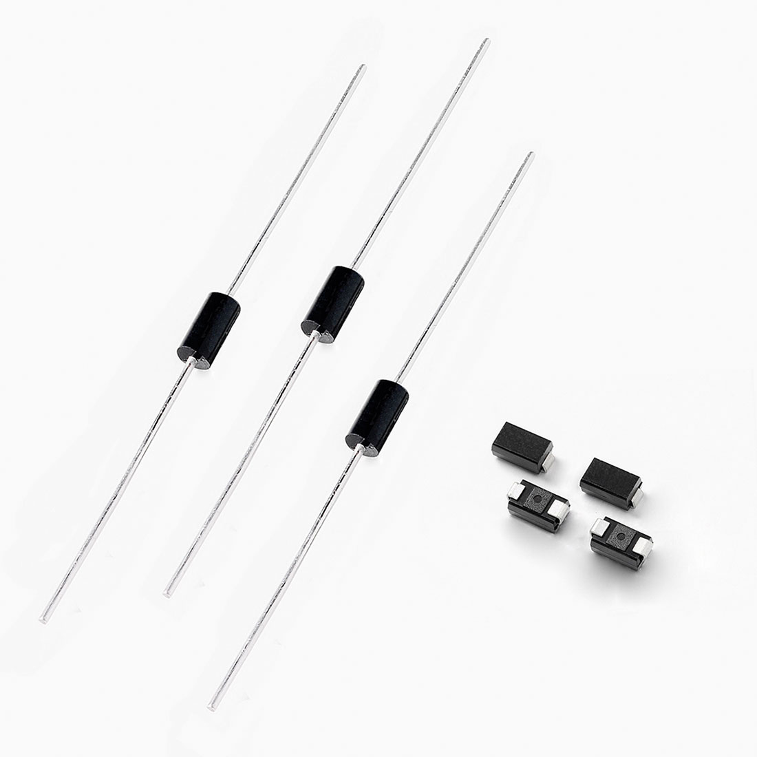
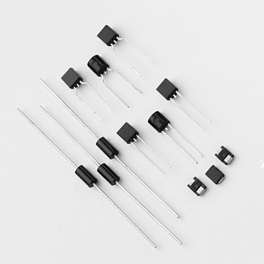
Diodes, Transistors, Thyristors, ICs & Valves
Diodes, Transistors, Thyristors, ICs & Valves
Diodes, Transistors, Thyristors, ICs & Valves
Diodes, Transistors, Thyristors, ICs & Valves
Diodes, Transistors, Thyristors, ICs & Valves
Diodes, Transistors, Thyristors, ICs & Valves
Diodes, Transistors, Thyristors, ICs & Valves
Diodes, Transistors, Thyristors, ICs & Valves
Diodes, Transistors, Thyristors, ICs & Valves
| DIODES · TRANSISTORS INTEGRATED CIRCUITS · THYRISTORS THERMIONIC VALVES · IDENTITY |
| DIODES · TRANSISTORS INTEGRATED CIRCUITS · THYRISTORS THERMIONIC VALVES · IDENTITY |
| DIODES · TRANSISTORS INTEGRATED CIRCUITS · THYRISTORS THERMIONIC VALVES · IDENTITY |
| DIODES · TRANSISTORS INTEGRATED CIRCUITS · THYRISTORS THERMIONIC VALVES · IDENTITY |
| DIODES · TRANSISTORS INTEGRATED CIRCUITS · THYRISTORS THERMIONIC VALVES · IDENTITY |
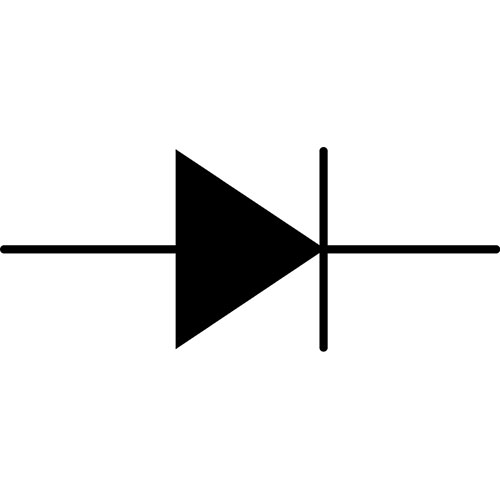
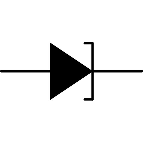
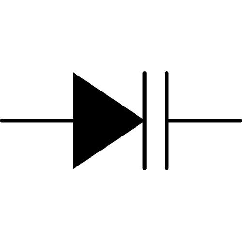
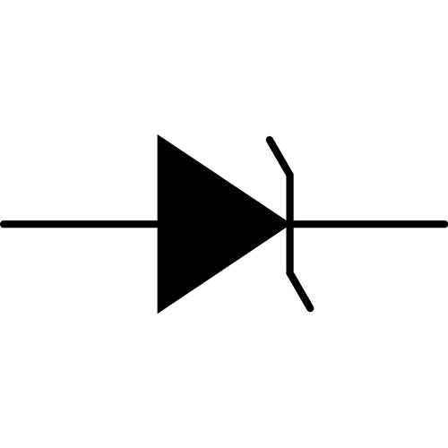
| Includes: Constant Current, DIAC, Fast Recovery, Gunn, Laser, Light Emitting, Photo, PIN, Power, Schottky Barrier, Shockley, SIDAC, Signal, Tunnel, TVS, Varactor, Varistor, Zener & Full Bridge Rectifier. Definition: Diodes of all types share one common feature, to allow for the transfer of current in one direction only, from the Anode to the Cathode, known as asymmetric conductance. Diodes are principally used for rectifying waveforms within power supplies, radio detectors and many application specific tasks from logic gates to oscillators. Made mostly from semiconductors such as silicon or germanium, all diodes types transmit electrical current in one direction, yet possess secondary characteristics, from maintaining constant currents, suppressing transient voltages to the ability of emitting light. History: In 1876, Karl Ferdinand Braun, Physicist, discovered this effect as he discovered current passing in one direction only. Then, in 1904, Sir John Fleming created the vacuum tube diode, the thermionic diode with a plate for the anode and a heated element as the cathode. Diodes of today mimic the device made of selenium and germanium, when in 1939, the discovery of a “PN Junction” device by Electrical Engineer, Russell Ohl, led to the domination of solid state silicon barrier diodes. |
| Includes: Constant Current, DIAC, Fast Recovery, Gunn, Laser, Light Emitting, Photo, PIN, Power, Schottky Barrier, Shockley, SIDAC, Signal, Tunnel, TVS, Varactor, Varistor, Zener & Full Bridge Rectifier. Definition: Diodes of all types share one common feature, to allow for the transfer of current in one direction only, from the Anode to the Cathode, known as asymmetric conductance. Diodes are principally used for rectifying waveforms within power supplies, radio detectors and many application specific tasks from logic gates to oscillators. Made mostly from semiconductors such as silicon or germanium, all diodes types transmit electrical current in one direction, yet possess secondary characteristics, from maintaining constant currents, suppressing transient voltages to the ability of emitting light. History: In 1876, Karl Ferdinand Braun, Physicist, discovered this effect as he discovered current passing in one direction only. Then, in 1904, Sir John Fleming created the vacuum tube diode, the thermionic diode with a plate for the anode and a heated element as the cathode. Diodes of today mimic the device made of selenium and germanium, when in 1939, the discovery of a “PN Junction” device by Electrical Engineer, Russell Ohl, led to the domination of solid state silicon barrier diodes. |
| Includes: Constant Current, DIAC, Fast Recovery, Gunn, Laser, Light Emitting, Photo, PIN, Power, Schottky Barrier, Shockley, SIDAC, Signal, Tunnel, TVS, Varactor, Varistor, Zener & Full Bridge Rectifier. Definition: Diodes of all types share one common feature, to allow for the transfer of current in one direction only, from the Anode to the Cathode, known as asymmetric conductance. Diodes are principally used for rectifying waveforms within power supplies, radio detectors and many application specific tasks from logic gates to oscillators. Made mostly from semiconductors such as silicon or germanium, all diodes types transmit electrical current in one direction, yet possess secondary characteristics, from maintaining constant currents, suppressing transient voltages to the ability of emitting light. History: In 1876, Karl Ferdinand Braun, Physicist, discovered this effect as he discovered current passing in one direction only. Then, in 1904, Sir John Fleming created the vacuum tube diode, the thermionic diode with a plate for the anode and a heated element as the cathode. Diodes of today mimic the device made of selenium and germanium, when in 1939, the discovery of a “PN Junction” device by Electrical Engineer, Russell Ohl, led to the domination of solid state silicon barrier diodes. |
| Includes: Constant Current, DIAC, Fast Recovery, Gunn, Laser, Light Emitting, Photo, PIN, Power, Schottky Barrier, Shockley, SIDAC, Signal, Tunnel, TVS, Varactor, Varistor, Zener & Full Bridge Rectifier. Definition: Diodes of all types share one common feature, to allow for the transfer of current in one direction only, from the Anode to the Cathode, known as asymmetric conductance. Diodes are principally used for rectifying waveforms within power supplies, radio detectors and many application specific tasks from logic gates to oscillators. Made mostly from semiconductors such as silicon or germanium, all diodes types transmit electrical current in one direction, yet possess secondary characteristics, from maintaining constant currents, suppressing transient voltages to the ability of emitting light. History: In 1876, Karl Ferdinand Braun, Physicist, discovered this effect as he discovered current passing in one direction only. Then, in 1904, Sir John Fleming created the vacuum tube diode, the thermionic diode with a plate for the anode and a heated element as the cathode. Diodes of today mimic the device made of selenium and germanium, when in 1939, the discovery of a “PN Junction” device by Electrical Engineer, Russell Ohl, led to the domination of solid state silicon barrier diodes. |
| Includes: Constant Current, DIAC, Fast Recovery, Gunn, Laser, Light Emitting, Photo, PIN, Power, Schottky Barrier, Shockley, SIDAC, Signal, Tunnel, TVS, Varactor, Varistor, Zener & Full Bridge Rectifier. Definition: Diodes of all types share one common feature, to allow for the transfer of current in one direction only, from the Anode to the Cathode, known as asymmetric conductance. Diodes are principally used for rectifying waveforms within power supplies, radio detectors and many application specific tasks from logic gates to oscillators. Made mostly from semiconductors such as silicon or germanium, all diodes types transmit electrical current in one direction, yet possess secondary characteristics, from maintaining constant currents, suppressing transient voltages to the ability of emitting light. History: In 1876, Karl Ferdinand Braun, Physicist, discovered this effect as he discovered current passing in one direction only. Then, in 1904, Sir John Fleming created the vacuum tube diode, the thermionic diode with a plate for the anode and a heated element as the cathode. Diodes of today mimic the device made of selenium and germanium, when in 1939, the discovery of a “PN Junction” device by Electrical Engineer, Russell Ohl, led to the domination of solid state silicon barrier diodes. |
| Invented in 1904 by Sir John Ambrose Fleming. |
| Invented in 1904 by Sir John Ambrose Fleming. |
| Invented in 1904 by Sir John Ambrose Fleming. |
| Invented in 1904 by Sir John Ambrose Fleming. |
| Invented in 1904 by Sir John Ambrose Fleming. |
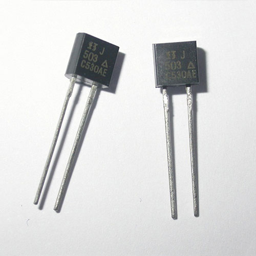
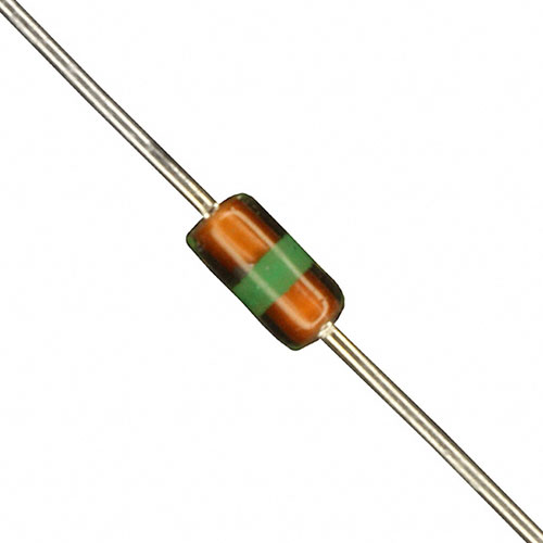
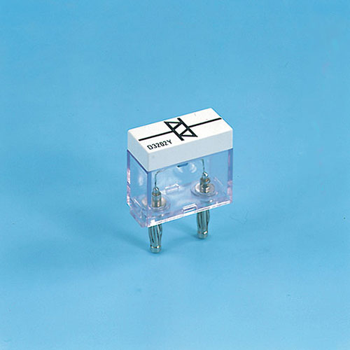
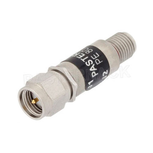
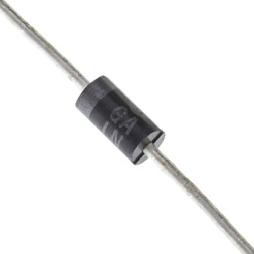
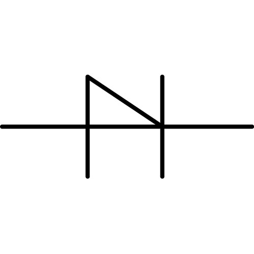
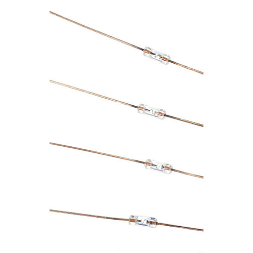
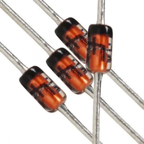
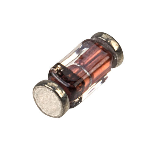
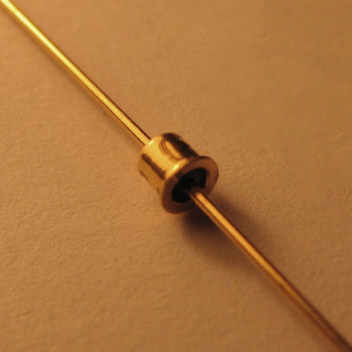
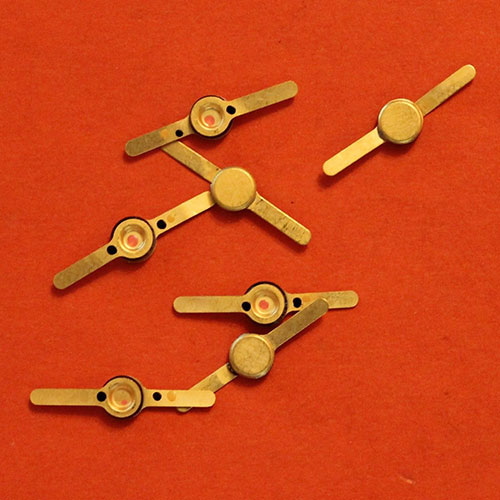
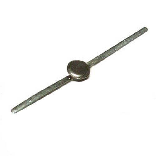
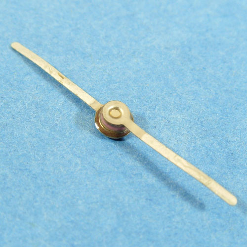
| Diode, Constant Current |
| Diode, Constant Current |
| Diode, Constant Current |
| Diode, Constant Current |
| Diode, Constant Current |
 |
|
|
|
|
| Definition: Constant Current Diodes, aka the current limiting diode, current regulating diode or diode connected transistor, these diodes regulate current over a wide voltage range and allow this current to pass through them, rise, then level off, maintaining a constant current. An n-channel JFET transistor with the gate shorted to the source can function as a replacement. |
| Definition: Constant Current Diodes, aka the current limiting diode, current regulating diode or diode connected transistor, these diodes regulate current over a wide voltage range and allow this current to pass through them, rise, then level off, maintaining a constant current. An n-channel JFET transistor with the gate shorted to the source can function as a replacement. |
| Definition: Constant Current Diodes, aka the current limiting diode, current regulating diode or diode connected transistor, these diodes regulate current over a wide voltage range and allow this current to pass through them, rise, then level off, maintaining a constant current. An n-channel JFET transistor with the gate shorted to the source can function as a replacement. |
| Definition: Constant Current Diodes, aka the current limiting diode, current regulating diode or diode connected transistor, these diodes regulate current over a wide voltage range and allow this current to pass through them, rise, then level off, maintaining a constant current. An n-channel JFET transistor with the gate shorted to the source can function as a replacement. |
| Definition: Constant Current Diodes, aka the current limiting diode, current regulating diode or diode connected transistor, these diodes regulate current over a wide voltage range and allow this current to pass through them, rise, then level off, maintaining a constant current. An n-channel JFET transistor with the gate shorted to the source can function as a replacement. |
 |
 |
 |
 |
|
|
|
|
|
|
|
|
|
|
|
|
|
|
|
|
| Invented in 1947 by William Bradford Shockley. |
| Invented in 1947 by William Bradford Shockley. |
| Invented in 1947 by William Bradford Shockley. |
| Invented in 1947 by William Bradford Shockley. |
| Invented in 1947 by William Bradford Shockley. |
 |
|
|
|
|
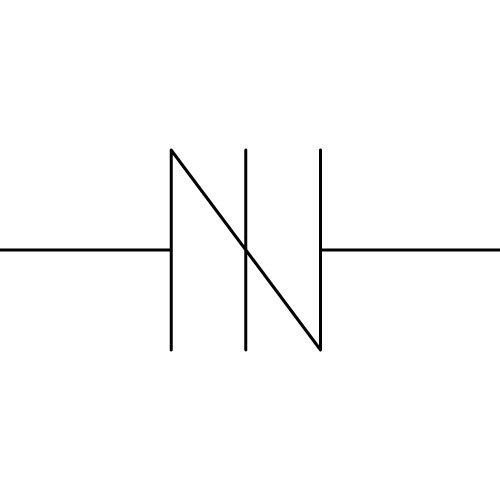
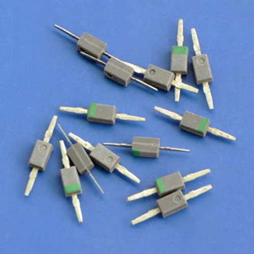
| Definition: The DIAC, known as the diode for alternating current, share characteristics to the SIDAC and are a bidirectional diode has two terminals labelled as A1 and A2 or MT1 and MT2. Commonly used as triggers for TRIAC devices, it will only conduct electrical current after its breakover voltage, VBO, has been momentarily reached, then enters a region of negative dynamic resistance that leads to a decrease in the voltage drop across the diode and an increase in current. Conduction remains until the current drops below the holding current, IH and resumes its high-resistance, non-conducting state. |
| Definition: The DIAC, known as the diode for alternating current, share characteristics to the SIDAC and are a bidirectional diode has two terminals labelled as A1 and A2 or MT1 and MT2. Commonly used as triggers for TRIAC devices, it will only conduct electrical current after its breakover voltage, VBO, has been momentarily reached, then enters a region of negative dynamic resistance that leads to a decrease in the voltage drop across the diode and an increase in current. Conduction remains until the current drops below the holding current, IH and resumes its high-resistance, non-conducting state. |
| Definition: The DIAC, known as the diode for alternating current, share characteristics to the SIDAC and are a bidirectional diode has two terminals labelled as A1 and A2 or MT1 and MT2. Commonly used as triggers for TRIAC devices, it will only conduct electrical current after its breakover voltage, VBO, has been momentarily reached, then enters a region of negative dynamic resistance that leads to a decrease in the voltage drop across the diode and an increase in current. Conduction remains until the current drops below the holding current, IH and resumes its high-resistance, non-conducting state. |
| Definition: The DIAC, known as the diode for alternating current, share characteristics to the SIDAC and are a bidirectional diode has two terminals labelled as A1 and A2 or MT1 and MT2. Commonly used as triggers for TRIAC devices, it will only conduct electrical current after its breakover voltage, VBO, has been momentarily reached, then enters a region of negative dynamic resistance that leads to a decrease in the voltage drop across the diode and an increase in current. Conduction remains until the current drops below the holding current, IH and resumes its high-resistance, non-conducting state. |
| Definition: The DIAC, known as the diode for alternating current, share characteristics to the SIDAC and are a bidirectional diode has two terminals labelled as A1 and A2 or MT1 and MT2. Commonly used as triggers for TRIAC devices, it will only conduct electrical current after its breakover voltage, VBO, has been momentarily reached, then enters a region of negative dynamic resistance that leads to a decrease in the voltage drop across the diode and an increase in current. Conduction remains until the current drops below the holding current, IH and resumes its high-resistance, non-conducting state. |
 |
 |
 |
 |
|
|
|
|
|
|
|
|
|
|
|
|
|
|
|
|
| Invented in 1958 by Richard Aldrich & Nick Holonyak. |
| Invented in 1958 by Richard Aldrich & Nick Holonyak. |
| Invented in 1958 by Richard Aldrich & Nick Holonyak. |
| Invented in 1958 by Richard Aldrich & Nick Holonyak. |
| Invented in 1958 by Richard Aldrich & Nick Holonyak. |
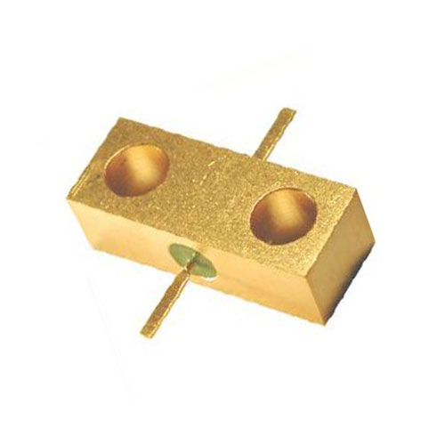
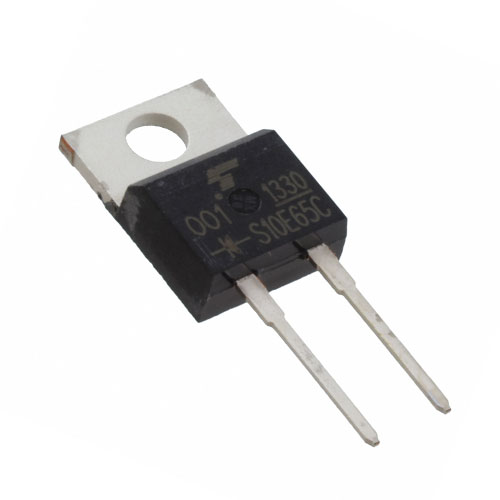
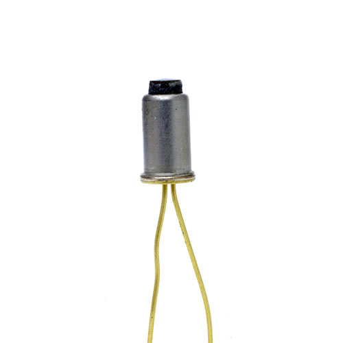
| Diode, Fast Recovery |
| Diode, Fast Recovery |
| Diode, Fast Recovery |
| Diode, Fast Recovery |
| Diode, Fast Recovery |
 |
|
|
|
|
| Definition: Fast recovery diodes are the requirement of every GTO, IGCT or IGBT (for “free-wheeling” reactive power) in order to enable operation of the DC-AC conversion system with inductive loads. Fast Recovery diodes are optimised to accept high dynamic stress (fast transition from conducting to blocking state) and generally have higher conduction losses than rectifier diodes. |
| Definition: Fast recovery diodes are the requirement of every GTO, IGCT or IGBT (for “free-wheeling” reactive power) in order to enable operation of the DC-AC conversion system with inductive loads. Fast Recovery diodes are optimised to accept high dynamic stress (fast transition from conducting to blocking state) and generally have higher conduction losses than rectifier diodes. |
| Definition: Fast recovery diodes are the requirement of every GTO, IGCT or IGBT (for “free-wheeling” reactive power) in order to enable operation of the DC-AC conversion system with inductive loads. Fast Recovery diodes are optimised to accept high dynamic stress (fast transition from conducting to blocking state) and generally have higher conduction losses than rectifier diodes. |
| Definition: Fast recovery diodes are the requirement of every GTO, IGCT or IGBT (for “free-wheeling” reactive power) in order to enable operation of the DC-AC conversion system with inductive loads. Fast Recovery diodes are optimised to accept high dynamic stress (fast transition from conducting to blocking state) and generally have higher conduction losses than rectifier diodes. |
| Definition: Fast recovery diodes are the requirement of every GTO, IGCT or IGBT (for “free-wheeling” reactive power) in order to enable operation of the DC-AC conversion system with inductive loads. Fast Recovery diodes are optimised to accept high dynamic stress (fast transition from conducting to blocking state) and generally have higher conduction losses than rectifier diodes. |
 |
 |
 |
 |
|
|
|
|
|
|
|
|
|
|
|
|
|
|
|
|
| Invented in 1950 by Jun-ichi Nishizawa. |
| Invented in 1950 by Jun-ichi Nishizawa. |
| Invented in 1950 by Jun-ichi Nishizawa. |
| Invented in 1950 by Jun-ichi Nishizawa. |
| Invented in 1950 by Jun-ichi Nishizawa. |
 |
|
|
|
|
| Definition: Gunn diodes are used to build oscillators for generating microwaves with frequencies ranging from 10 Gigahertz to Terahertz. It is a Negative Differential Resistance device, also known as a transferred electron device oscillator, which is a tuned circuit consisting of Gunn diode with DC bias voltage applied to it. Due to this, the total differential resistance of the circuit becomes zero as the negative resistance of the diode cancels with the positive resistance of the circuit resulting in the generation of oscillations. This diode is made of materials like GaAs or InP that exhibit a negative differential resistance region. |
| Definition: Gunn diodes are used to build oscillators for generating microwaves with frequencies ranging from 10 Gigahertz to Terahertz. It is a Negative Differential Resistance device, also known as a transferred electron device oscillator, which is a tuned circuit consisting of Gunn diode with DC bias voltage applied to it. Due to this, the total differential resistance of the circuit becomes zero as the negative resistance of the diode cancels with the positive resistance of the circuit resulting in the generation of oscillations. This diode is made of materials like GaAs or InP that exhibit a negative differential resistance region. |
| Definition: Gunn diodes are used to build oscillators for generating microwaves with frequencies ranging from 10 Gigahertz to Terahertz. It is a Negative Differential Resistance device, also known as a transferred electron device oscillator, which is a tuned circuit consisting of Gunn diode with DC bias voltage applied to it. Due to this, the total differential resistance of the circuit becomes zero as the negative resistance of the diode cancels with the positive resistance of the circuit resulting in the generation of oscillations. This diode is made of materials like GaAs or InP that exhibit a negative differential resistance region. |
| Definition: Gunn diodes are used to build oscillators for generating microwaves with frequencies ranging from 10 Gigahertz to Terahertz. It is a Negative Differential Resistance device, also known as a transferred electron device oscillator, which is a tuned circuit consisting of Gunn diode with DC bias voltage applied to it. Due to this, the total differential resistance of the circuit becomes zero as the negative resistance of the diode cancels with the positive resistance of the circuit resulting in the generation of oscillations. This diode is made of materials like GaAs or InP that exhibit a negative differential resistance region. |
| Definition: Gunn diodes are used to build oscillators for generating microwaves with frequencies ranging from 10 Gigahertz to Terahertz. It is a Negative Differential Resistance device, also known as a transferred electron device oscillator, which is a tuned circuit consisting of Gunn diode with DC bias voltage applied to it. Due to this, the total differential resistance of the circuit becomes zero as the negative resistance of the diode cancels with the positive resistance of the circuit resulting in the generation of oscillations. This diode is made of materials like GaAs or InP that exhibit a negative differential resistance region. |
 |
 |
 |
 |
|
|
|
|
|
|
|
|
|
|
|
|
|
|
|
|
| Invented in 1962 by John Battiscombe (J B) Gunn. |
| Invented in 1962 by John Battiscombe (J B) Gunn. |
| Invented in 1962 by John Battiscombe (J B) Gunn. |
| Invented in 1962 by John Battiscombe (J B) Gunn. |
| Invented in 1962 by John Battiscombe (J B) Gunn. |
 |
|
|
|
|
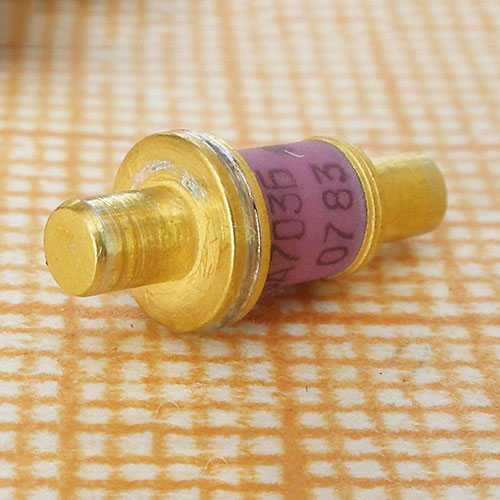
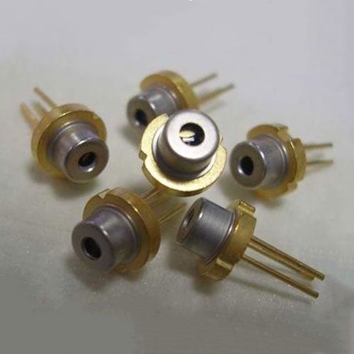
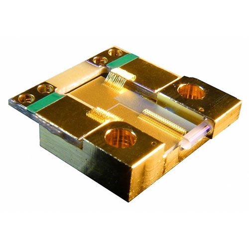
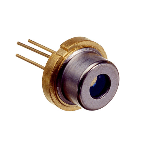
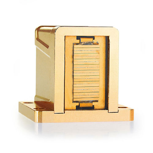
| Definition: Laser Diodes are different from LED types, as this diode produces coherent light and find their application in DVD and CD drives, laser pointers. They are edge-emitting lasers, whereby a laser resonator is formed by coating the end facets of a semiconductor wafer, restricting the generated carriers to a narrow region, providing a waveguide for the optical field. The current flow is restricted in this region, leading to relatively low threshold pump power and high efficiency. This active region is usually quite thin, acting as a quantum well. Modern laser diodes are surface-emitting and directed perpendicular to the wafer surface, resulting in the gain provided by multiple quantum wells. |
| Definition: Laser Diodes are different from LED types, as this diode produces coherent light and find their application in DVD and CD drives, laser pointers. They are edge-emitting lasers, whereby a laser resonator is formed by coating the end facets of a semiconductor wafer, restricting the generated carriers to a narrow region, providing a waveguide for the optical field. The current flow is restricted in this region, leading to relatively low threshold pump power and high efficiency. This active region is usually quite thin, acting as a quantum well. Modern laser diodes are surface-emitting and directed perpendicular to the wafer surface, resulting in the gain provided by multiple quantum wells. |
| Definition: Laser Diodes are different from LED types, as this diode produces coherent light and find their application in DVD and CD drives, laser pointers. They are edge-emitting lasers, whereby a laser resonator is formed by coating the end facets of a semiconductor wafer, restricting the generated carriers to a narrow region, providing a waveguide for the optical field. The current flow is restricted in this region, leading to relatively low threshold pump power and high efficiency. This active region is usually quite thin, acting as a quantum well. Modern laser diodes are surface-emitting and directed perpendicular to the wafer surface, resulting in the gain provided by multiple quantum wells. |
| Definition: Laser Diodes are different from LED types, as this diode produces coherent light and find their application in DVD and CD drives, laser pointers. They are edge-emitting lasers, whereby a laser resonator is formed by coating the end facets of a semiconductor wafer, restricting the generated carriers to a narrow region, providing a waveguide for the optical field. The current flow is restricted in this region, leading to relatively low threshold pump power and high efficiency. This active region is usually quite thin, acting as a quantum well. Modern laser diodes are surface-emitting and directed perpendicular to the wafer surface, resulting in the gain provided by multiple quantum wells. |
| Definition: Laser Diodes are different from LED types, as this diode produces coherent light and find their application in DVD and CD drives, laser pointers. They are edge-emitting lasers, whereby a laser resonator is formed by coating the end facets of a semiconductor wafer, restricting the generated carriers to a narrow region, providing a waveguide for the optical field. The current flow is restricted in this region, leading to relatively low threshold pump power and high efficiency. This active region is usually quite thin, acting as a quantum well. Modern laser diodes are surface-emitting and directed perpendicular to the wafer surface, resulting in the gain provided by multiple quantum wells. |
 |
 |
 |
 |
|
|
|
|
|
|
|
|
|
|
|
|
|
|
|
|
| Invented in 1957 by Jun-ichi Nishizawa. |
| Invented in 1957 by Jun-ichi Nishizawa. |
| Invented in 1957 by Jun-ichi Nishizawa. |
| Invented in 1957 by Jun-ichi Nishizawa. |
| Invented in 1957 by Jun-ichi Nishizawa. |
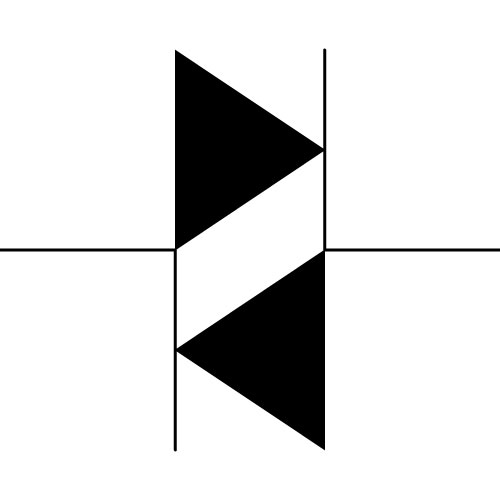
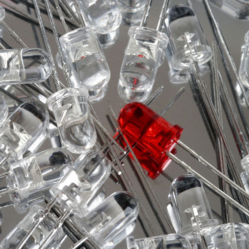
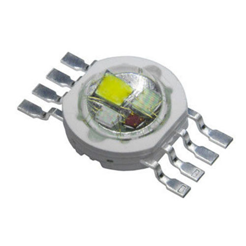
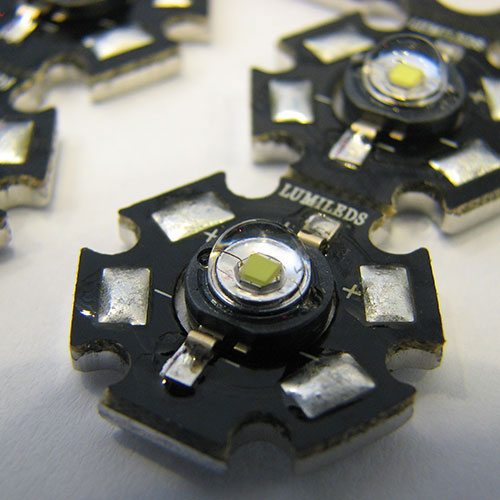
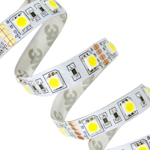
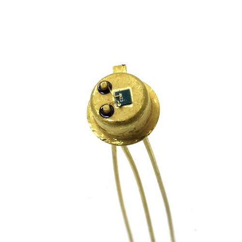
| Diode, Light Emitting |
| Diode, Light Emitting |
| Diode, Light Emitting |
| Diode, Light Emitting |
| Diode, Light Emitting |
 |
|
|
|
|
| Definition: Light emitting diodes, known as LEDs, permits the transfer of electric current between electrodes to produce light. When switched on or forward biased, the electrons recombine with the holes and release energy in the form of light, the colour of which is determined by the energy gap of the semiconductor. The first LED was an infrared light emission from a tunnel diode constructed on gallium arsenide (GaAs) semi-insulating substrate. The first visible light from an LED, was red in colour and invented in 1962 by Electrical Engineer, Nick Holonyak. |
| Definition: Light emitting diodes, known as LEDs, permits the transfer of electric current between electrodes to produce light. When switched on or forward biased, the electrons recombine with the holes and release energy in the form of light, the colour of which is determined by the energy gap of the semiconductor. The first LED was an infrared light emission from a tunnel diode constructed on gallium arsenide (GaAs) semi-insulating substrate. The first visible light from an LED, was red in colour and invented in 1962 by Electrical Engineer, Nick Holonyak. |
| Definition: Light emitting diodes, known as LEDs, permits the transfer of electric current between electrodes to produce light. When switched on or forward biased, the electrons recombine with the holes and release energy in the form of light, the colour of which is determined by the energy gap of the semiconductor. The first LED was an infrared light emission from a tunnel diode constructed on gallium arsenide (GaAs) semi-insulating substrate. The first visible light from an LED, was red in colour and invented in 1962 by Electrical Engineer, Nick Holonyak. |
| Definition: Light emitting diodes, known as LEDs, permits the transfer of electric current between electrodes to produce light. When switched on or forward biased, the electrons recombine with the holes and release energy in the form of light, the colour of which is determined by the energy gap of the semiconductor. The first LED was an infrared light emission from a tunnel diode constructed on gallium arsenide (GaAs) semi-insulating substrate. The first visible light from an LED, was red in colour and invented in 1962 by Electrical Engineer, Nick Holonyak. |
| Definition: Light emitting diodes, known as LEDs, permits the transfer of electric current between electrodes to produce light. When switched on or forward biased, the electrons recombine with the holes and release energy in the form of light, the colour of which is determined by the energy gap of the semiconductor. The first LED was an infrared light emission from a tunnel diode constructed on gallium arsenide (GaAs) semi-insulating substrate. The first visible light from an LED, was red in colour and invented in 1962 by Electrical Engineer, Nick Holonyak. |
 |
 |
 |
 |
|
|
|
|
|
|
|
|
|
|
|
|
|
|
|
|
| Invented in 1961 by James (Bob) Biard & Gary Edmund Pittman. |
| Invented in 1961 by James (Bob) Biard & Gary Edmund Pittman. |
| Invented in 1961 by James (Bob) Biard & Gary Edmund Pittman. |
| Invented in 1961 by James (Bob) Biard & Gary Edmund Pittman. |
| Invented in 1961 by James (Bob) Biard & Gary Edmund Pittman. |
 |
|
|
|
|
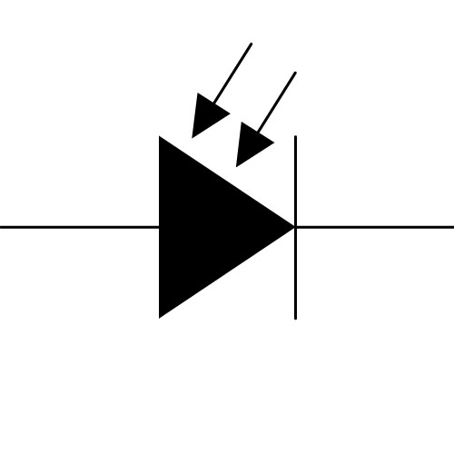
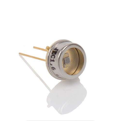
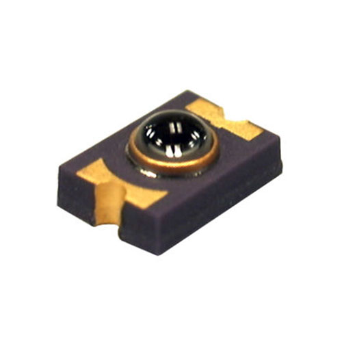
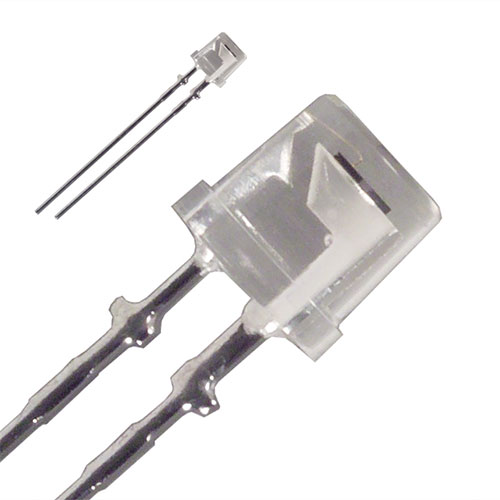
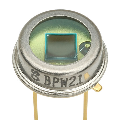
| Definition: The invention of the photo diode shares characteristics with Solar and Photovoltaic Cells, PN, PIN Diodes, Photo Transistors, Thyristors and FETS, by converting light directly into electricity and are photovoltaic in sun or artificial light. This invention, improved upon in sensitivity and capacity with the Avalanche Photo Diode, invented in 1952 by Jun-ichi Nishizawa, will instigate an electron-hole pair avalanche breakdown, which will create more than 100 electron-hole pairs per electron event, creating a sensitive detector for use in fibre optical communication, high-speed laser scanning and imaging. |
| Definition: The invention of the photo diode shares characteristics with Solar and Photovoltaic Cells, PN, PIN Diodes, Photo Transistors, Thyristors and FETS, by converting light directly into electricity and are photovoltaic in sun or artificial light. This invention, improved upon in sensitivity and capacity with the Avalanche Photo Diode, invented in 1952 by Jun-ichi Nishizawa, will instigate an electron-hole pair avalanche breakdown, which will create more than 100 electron-hole pairs per electron event, creating a sensitive detector for use in fibre optical communication, high-speed laser scanning and imaging. |
| Definition: The invention of the photo diode shares characteristics with Solar and Photovoltaic Cells, PN, PIN Diodes, Photo Transistors, Thyristors and FETS, by converting light directly into electricity and are photovoltaic in sun or artificial light. This invention, improved upon in sensitivity and capacity with the Avalanche Photo Diode, invented in 1952 by Jun-ichi Nishizawa, will instigate an electron-hole pair avalanche breakdown, which will create more than 100 electron-hole pairs per electron event, creating a sensitive detector for use in fibre optical communication, high-speed laser scanning and imaging. |
| Definition: The invention of the photo diode shares characteristics with Solar and Photovoltaic Cells, PN, PIN Diodes, Photo Transistors, Thyristors and FETS, by converting light directly into electricity and are photovoltaic in sun or artificial light. This invention, improved upon in sensitivity and capacity with the Avalanche Photo Diode, invented in 1952 by Jun-ichi Nishizawa, will instigate an electron-hole pair avalanche breakdown, which will create more than 100 electron-hole pairs per electron event, creating a sensitive detector for use in fibre optical communication, high-speed laser scanning and imaging. |
| Definition: The invention of the photo diode shares characteristics with Solar and Photovoltaic Cells, PN, PIN Diodes, Photo Transistors, Thyristors and FETS, by converting light directly into electricity and are photovoltaic in sun or artificial light. This invention, improved upon in sensitivity and capacity with the Avalanche Photo Diode, invented in 1952 by Jun-ichi Nishizawa, will instigate an electron-hole pair avalanche breakdown, which will create more than 100 electron-hole pairs per electron event, creating a sensitive detector for use in fibre optical communication, high-speed laser scanning and imaging. |
 |
 |
 |
 |
|
|
|
|
|
|
|
|
|
|
|
|
|
|
|
|
| Invented in 1952 by Jun-ichi Nishizawa. |
| Invented in 1952 by Jun-ichi Nishizawa. |
| Invented in 1952 by Jun-ichi Nishizawa. |
| Invented in 1952 by Jun-ichi Nishizawa. |
| Invented in 1952 by Jun-ichi Nishizawa. |
 |
|
|
|
|
| Definition: Pin diodes are formed with a central un-doped, or intrinsic, layer, forming a p-type/intrinsic/n-type structure, these diodes are used for radio frequency switches, attenuators, ionising-radiation detectors and photodetectors. Used in power electronics, their central layer can withstand high voltages. This PIN structure underpins many power semiconductor devices, such as IGBTs, power MOSFETs, and thyristors. |
| Definition: Pin diodes are formed with a central un-doped, or intrinsic, layer, forming a p-type/intrinsic/n-type structure, these diodes are used for radio frequency switches, attenuators, ionising-radiation detectors and photodetectors. Used in power electronics, their central layer can withstand high voltages. This PIN structure underpins many power semiconductor devices, such as IGBTs, power MOSFETs, and thyristors. |
| Definition: Pin diodes are formed with a central un-doped, or intrinsic, layer, forming a p-type/intrinsic/n-type structure, these diodes are used for radio frequency switches, attenuators, ionising-radiation detectors and photodetectors. Used in power electronics, their central layer can withstand high voltages. This PIN structure underpins many power semiconductor devices, such as IGBTs, power MOSFETs, and thyristors. |
| Definition: Pin diodes are formed with a central un-doped, or intrinsic, layer, forming a p-type/intrinsic/n-type structure, these diodes are used for radio frequency switches, attenuators, ionising-radiation detectors and photodetectors. Used in power electronics, their central layer can withstand high voltages. This PIN structure underpins many power semiconductor devices, such as IGBTs, power MOSFETs, and thyristors. |
| Definition: Pin diodes are formed with a central un-doped, or intrinsic, layer, forming a p-type/intrinsic/n-type structure, these diodes are used for radio frequency switches, attenuators, ionising-radiation detectors and photodetectors. Used in power electronics, their central layer can withstand high voltages. This PIN structure underpins many power semiconductor devices, such as IGBTs, power MOSFETs, and thyristors. |
 |
 |
 |
 |
|
|
|
|
|
|
|
|
|
|
|
|
|
|
|
|
| Invented in 1950 by Jun-ichi Nishizawa. |
| Invented in 1950 by Jun-ichi Nishizawa. |
| Invented in 1950 by Jun-ichi Nishizawa. |
| Invented in 1950 by Jun-ichi Nishizawa. |
| Invented in 1950 by Jun-ichi Nishizawa. |
 |
|
|
|
|
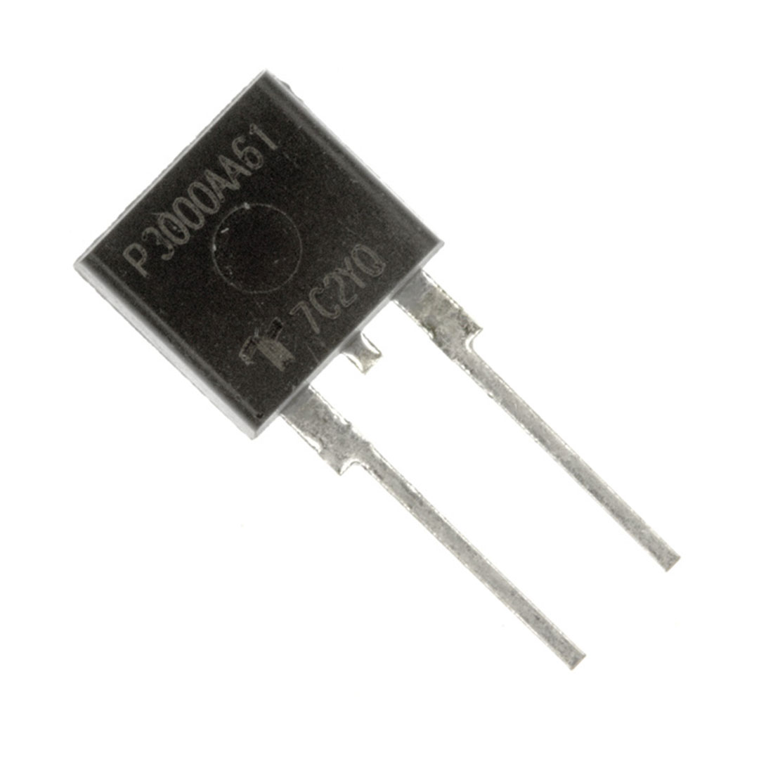
| Definition: Power diodes are used to rectify alternating power inputs in power supplies and in high-power applications, they are built with large P-N junctions in order to pass large amounts of current, dissipate large amounts of heat and withstand high voltages in reverse bias. There are many variations manufactured, from high current diodes, high voltage diodes, PN power diodes, PIN power diodes, RF power diodes, switching power diodes, and rectifier power diodes. |
| Definition: Power diodes are used to rectify alternating power inputs in power supplies and in high-power applications, they are built with large P-N junctions in order to pass large amounts of current, dissipate large amounts of heat and withstand high voltages in reverse bias. There are many variations manufactured, from high current diodes, high voltage diodes, PN power diodes, PIN power diodes, RF power diodes, switching power diodes, and rectifier power diodes. |
| Definition: Power diodes are used to rectify alternating power inputs in power supplies and in high-power applications, they are built with large P-N junctions in order to pass large amounts of current, dissipate large amounts of heat and withstand high voltages in reverse bias. There are many variations manufactured, from high current diodes, high voltage diodes, PN power diodes, PIN power diodes, RF power diodes, switching power diodes, and rectifier power diodes. |
| Definition: Power diodes are used to rectify alternating power inputs in power supplies and in high-power applications, they are built with large P-N junctions in order to pass large amounts of current, dissipate large amounts of heat and withstand high voltages in reverse bias. There are many variations manufactured, from high current diodes, high voltage diodes, PN power diodes, PIN power diodes, RF power diodes, switching power diodes, and rectifier power diodes. |
| Definition: Power diodes are used to rectify alternating power inputs in power supplies and in high-power applications, they are built with large P-N junctions in order to pass large amounts of current, dissipate large amounts of heat and withstand high voltages in reverse bias. There are many variations manufactured, from high current diodes, high voltage diodes, PN power diodes, PIN power diodes, RF power diodes, switching power diodes, and rectifier power diodes. |
 |
 |
 |
 |
|
|
|
|
|
|
|
|
|
|
|
|
|
|
|
|
| Invented in 1952 by Robert Hall. |
| Invented in 1952 by Robert Hall. |
| Invented in 1952 by Robert Hall. |
| Invented in 1952 by Robert Hall. |
| Invented in 1952 by Robert Hall. |
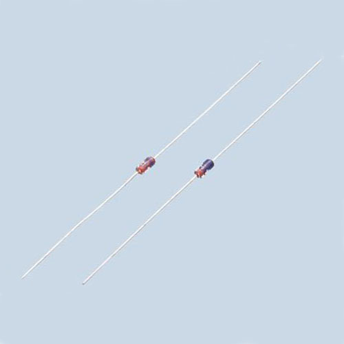
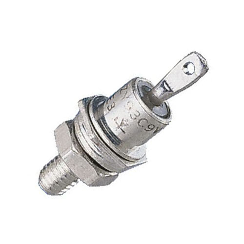
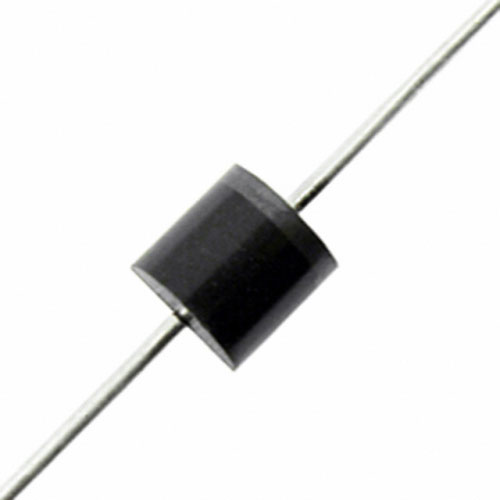
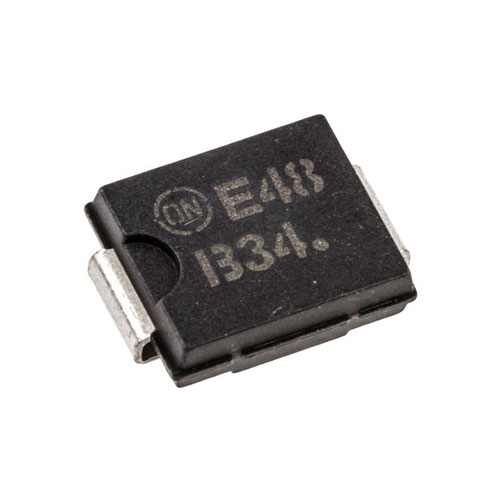
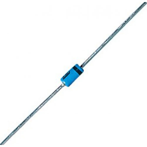
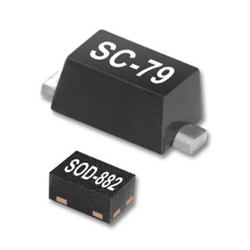
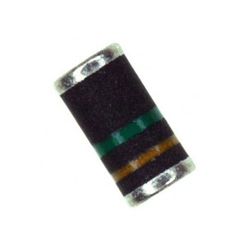
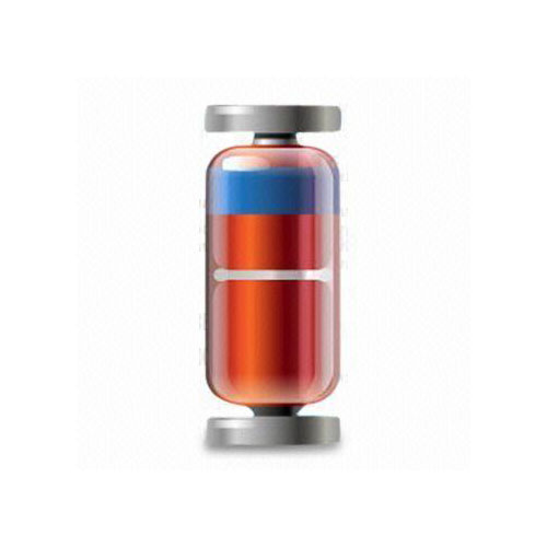
| Diode, Schottky Barrier |
| Diode, Schottky Barrier |
| Diode, Schottky Barrier |
| Diode, Schottky Barrier |
| Diode, Schottky Barrier |
 |
|
|
|
|
| Definition: Schottky diodes are named after German physicist Walter H. Schottky and are used in RF, rectifier and clamping applications, they feature a lower forward voltage drop as compared to the ordinary silicon PN junction diodes, from 150 millivolts to 400 millivolts at low currents, as compared to the 600 millivolts for a silicon diode. In order to achieve this performance, these diodes are constructed with a metal to semiconductor contact. |
| Definition: Schottky diodes are named after German physicist Walter H. Schottky and are used in RF, rectifier and clamping applications, they feature a lower forward voltage drop as compared to the ordinary silicon PN junction diodes, from 150 millivolts to 400 millivolts at low currents, as compared to the 600 millivolts for a silicon diode. In order to achieve this performance, these diodes are constructed with a metal to semiconductor contact. |
| Definition: Schottky diodes are named after German physicist Walter H. Schottky and are used in RF, rectifier and clamping applications, they feature a lower forward voltage drop as compared to the ordinary silicon PN junction diodes, from 150 millivolts to 400 millivolts at low currents, as compared to the 600 millivolts for a silicon diode. In order to achieve this performance, these diodes are constructed with a metal to semiconductor contact. |
| Definition: Schottky diodes are named after German physicist Walter H. Schottky and are used in RF, rectifier and clamping applications, they feature a lower forward voltage drop as compared to the ordinary silicon PN junction diodes, from 150 millivolts to 400 millivolts at low currents, as compared to the 600 millivolts for a silicon diode. In order to achieve this performance, these diodes are constructed with a metal to semiconductor contact. |
| Definition: Schottky diodes are named after German physicist Walter H. Schottky and are used in RF, rectifier and clamping applications, they feature a lower forward voltage drop as compared to the ordinary silicon PN junction diodes, from 150 millivolts to 400 millivolts at low currents, as compared to the 600 millivolts for a silicon diode. In order to achieve this performance, these diodes are constructed with a metal to semiconductor contact. |
 |
 |
 |
 |
|
|
|
|
|
|
|
|
|
|
|
|
|
|
|
|
| Invented in 1961 by James (Bob) Biard. |
| Invented in 1961 by James (Bob) Biard. |
| Invented in 1961 by James (Bob) Biard. |
| Invented in 1961 by James (Bob) Biard. |
| Invented in 1961 by James (Bob) Biard. |
 |
|
|
|
|
| Definition: Shockley diodes have four layers and is also known as the pnpn diode. It is equal to a thyristor without a gate terminal and as there is no trigger inputs the only way the diode can conduct is by providing a forward voltage. It stays on one’s it turned “ON” and stays off one’s it turned “OFF”. The diode has two operating states conducting and non-conducting. In non-conducting state the diode conducts with less voltage. |
| Definition: Shockley diodes have four layers and is also known as the pnpn diode. It is equal to a thyristor without a gate terminal and as there is no trigger inputs the only way the diode can conduct is by providing a forward voltage. It stays on one’s it turned “ON” and stays off one’s it turned “OFF”. The diode has two operating states conducting and non-conducting. In non-conducting state the diode conducts with less voltage. |
| Definition: Shockley diodes have four layers and is also known as the pnpn diode. It is equal to a thyristor without a gate terminal and as there is no trigger inputs the only way the diode can conduct is by providing a forward voltage. It stays on one’s it turned “ON” and stays off one’s it turned “OFF”. The diode has two operating states conducting and non-conducting. In non-conducting state the diode conducts with less voltage. |
| Definition: Shockley diodes have four layers and is also known as the pnpn diode. It is equal to a thyristor without a gate terminal and as there is no trigger inputs the only way the diode can conduct is by providing a forward voltage. It stays on one’s it turned “ON” and stays off one’s it turned “OFF”. The diode has two operating states conducting and non-conducting. In non-conducting state the diode conducts with less voltage. |
| Definition: Shockley diodes have four layers and is also known as the pnpn diode. It is equal to a thyristor without a gate terminal and as there is no trigger inputs the only way the diode can conduct is by providing a forward voltage. It stays on one’s it turned “ON” and stays off one’s it turned “OFF”. The diode has two operating states conducting and non-conducting. In non-conducting state the diode conducts with less voltage. |
 |
 |
 |
 |
|
|
|
|
|
|
|
|
|
|
|
|
|
|
|
|
| Invented in 1947 by William Bradford Shockley. |
| Invented in 1947 by William Bradford Shockley. |
| Invented in 1947 by William Bradford Shockley. |
| Invented in 1947 by William Bradford Shockley. |
| Invented in 1947 by William Bradford Shockley. |
 |
|
|
|
|
| Definition: SIDAC is a five-layer, silicon bilateral voltage triggered switch. When the voltage exceeds the SIDAC breakover voltage point, the SIDAC switches on and conduction continues until the current is interrupted or drops below the minimum holding current. SIDACs have glass-passivated junctions and are suitable for power supplies, gas igniters, high-pressure Sodium lamps and Xenon flash ignition. |
| Definition: SIDAC is a five-layer, silicon bilateral voltage triggered switch. When the voltage exceeds the SIDAC breakover voltage point, the SIDAC switches on and conduction continues until the current is interrupted or drops below the minimum holding current. SIDACs have glass-passivated junctions and are suitable for power supplies, gas igniters, high-pressure Sodium lamps and Xenon flash ignition. |
| Definition: SIDAC is a five-layer, silicon bilateral voltage triggered switch. When the voltage exceeds the SIDAC breakover voltage point, the SIDAC switches on and conduction continues until the current is interrupted or drops below the minimum holding current. SIDACs have glass-passivated junctions and are suitable for power supplies, gas igniters, high-pressure Sodium lamps and Xenon flash ignition. |
| Definition: SIDAC is a five-layer, silicon bilateral voltage triggered switch. When the voltage exceeds the SIDAC breakover voltage point, the SIDAC switches on and conduction continues until the current is interrupted or drops below the minimum holding current. SIDACs have glass-passivated junctions and are suitable for power supplies, gas igniters, high-pressure Sodium lamps and Xenon flash ignition. |
| Definition: SIDAC is a five-layer, silicon bilateral voltage triggered switch. When the voltage exceeds the SIDAC breakover voltage point, the SIDAC switches on and conduction continues until the current is interrupted or drops below the minimum holding current. SIDACs have glass-passivated junctions and are suitable for power supplies, gas igniters, high-pressure Sodium lamps and Xenon flash ignition. |
 |
 |
 |
 |
|
|
|
|
|
|
|
|
|
|
|
|
|
|
|
|
| Invented in 1965 by Jearld (Jerry) Hutson. |
| Invented in 1965 by Jearld (Jerry) Hutson. |
| Invented in 1965 by Jearld (Jerry) Hutson. |
| Invented in 1965 by Jearld (Jerry) Hutson. |
| Invented in 1965 by Jearld (Jerry) Hutson. |
 |
|
|
|
|
| Definition: Signal diodes are used in applications involving high frequency at very low currents, they are found in radios and televisions. With the junction enveloped in glass, it is also named as Glass Passivated Diode. This diode depends on the pressure of contact between a point and a semiconductor crystal for its operation. The diode consists of a small crystal of n-type silicon, with a fine beryllium-copper, bronze-phosphor, or tungsten wire (catwhisker) pressed against the crystal, forming the second part of the diode. During manufacture, a large current is passed from the catwhisker to the silicon crystal, resulting in the formation of a small region of p-type material around the crystal in the vicinity of the point contact, forming a pn-junction. This diode is commonly used in analogue applications and as a detector in radio receivers. |
| Definition: Signal diodes are used in applications involving high frequency at very low currents, they are found in radios and televisions. With the junction enveloped in glass, it is also named as Glass Passivated Diode. This diode depends on the pressure of contact between a point and a semiconductor crystal for its operation. The diode consists of a small crystal of n-type silicon, with a fine beryllium-copper, bronze-phosphor, or tungsten wire (catwhisker) pressed against the crystal, forming the second part of the diode. During manufacture, a large current is passed from the catwhisker to the silicon crystal, resulting in the formation of a small region of p-type material around the crystal in the vicinity of the point contact, forming a pn-junction. This diode is commonly used in analogue applications and as a detector in radio receivers. |
| Definition: Signal diodes are used in applications involving high frequency at very low currents, they are found in radios and televisions. With the junction enveloped in glass, it is also named as Glass Passivated Diode. This diode depends on the pressure of contact between a point and a semiconductor crystal for its operation. The diode consists of a small crystal of n-type silicon, with a fine beryllium-copper, bronze-phosphor, or tungsten wire (catwhisker) pressed against the crystal, forming the second part of the diode. During manufacture, a large current is passed from the catwhisker to the silicon crystal, resulting in the formation of a small region of p-type material around the crystal in the vicinity of the point contact, forming a pn-junction. This diode is commonly used in analogue applications and as a detector in radio receivers. |
| Definition: Signal diodes are used in applications involving high frequency at very low currents, they are found in radios and televisions. With the junction enveloped in glass, it is also named as Glass Passivated Diode. This diode depends on the pressure of contact between a point and a semiconductor crystal for its operation. The diode consists of a small crystal of n-type silicon, with a fine beryllium-copper, bronze-phosphor, or tungsten wire (catwhisker) pressed against the crystal, forming the second part of the diode. During manufacture, a large current is passed from the catwhisker to the silicon crystal, resulting in the formation of a small region of p-type material around the crystal in the vicinity of the point contact, forming a pn-junction. This diode is commonly used in analogue applications and as a detector in radio receivers. |
| Definition: Signal diodes are used in applications involving high frequency at very low currents, they are found in radios and televisions. With the junction enveloped in glass, it is also named as Glass Passivated Diode. This diode depends on the pressure of contact between a point and a semiconductor crystal for its operation. The diode consists of a small crystal of n-type silicon, with a fine beryllium-copper, bronze-phosphor, or tungsten wire (catwhisker) pressed against the crystal, forming the second part of the diode. During manufacture, a large current is passed from the catwhisker to the silicon crystal, resulting in the formation of a small region of p-type material around the crystal in the vicinity of the point contact, forming a pn-junction. This diode is commonly used in analogue applications and as a detector in radio receivers. |
 |
 |
 |
 |
|
|
|
|
|
|
|
|
|
|
|
|
|
|
|
|
| Invented in 1901 by Jagadis Chandra Bose. |
| Invented in 1901 by Jagadis Chandra Bose. |
| Invented in 1901 by Jagadis Chandra Bose. |
| Invented in 1901 by Jagadis Chandra Bose. |
| Invented in 1901 by Jagadis Chandra Bose. |
 |
|
|
|
|
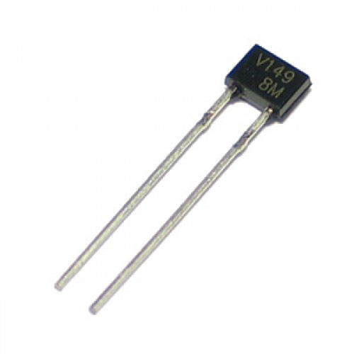
| Definition: Tunnel diodes have a region of operation, showing negative resistance caused by quantum tunnelling and allowing amplification of signals. Due to the high carrier concentration, tunnel diodes are very fast, may be used at very low temperatures, high magnetic fields and in high radiation environments. Because of these properties, they are often used in spacecraft. |
| Definition: Tunnel diodes have a region of operation, showing negative resistance caused by quantum tunnelling and allowing amplification of signals. Due to the high carrier concentration, tunnel diodes are very fast, may be used at very low temperatures, high magnetic fields and in high radiation environments. Because of these properties, they are often used in spacecraft. |
| Definition: Tunnel diodes have a region of operation, showing negative resistance caused by quantum tunnelling and allowing amplification of signals. Due to the high carrier concentration, tunnel diodes are very fast, may be used at very low temperatures, high magnetic fields and in high radiation environments. Because of these properties, they are often used in spacecraft. |
| Definition: Tunnel diodes have a region of operation, showing negative resistance caused by quantum tunnelling and allowing amplification of signals. Due to the high carrier concentration, tunnel diodes are very fast, may be used at very low temperatures, high magnetic fields and in high radiation environments. Because of these properties, they are often used in spacecraft. |
| Definition: Tunnel diodes have a region of operation, showing negative resistance caused by quantum tunnelling and allowing amplification of signals. Due to the high carrier concentration, tunnel diodes are very fast, may be used at very low temperatures, high magnetic fields and in high radiation environments. Because of these properties, they are often used in spacecraft. |
 |
 |
 |
 |
|
|
|
|
|
|
|
|
|
|
|
|
|
|
|
|
| Invented in 1958 by Leo Esaki. |
| Invented in 1958 by Leo Esaki. |
| Invented in 1958 by Leo Esaki. |
| Invented in 1958 by Leo Esaki. |
| Invented in 1958 by Leo Esaki. |
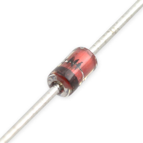
| Definition: Transient voltage suppression diodes, also known as a thyristor diode, operates by shunting excess current when the induced voltage exceeds the avalanche breakdown potential. It is a clamping device, suppressing all peaks above its breakdown voltage. It automatically resets when the overvoltage goes away, but absorbs much more of the transient energy internally than a similarly rated crowbar device. The transient-voltage-suppression diode may be either unidirectional or bidirectional. A unidirectional device operates as a rectifier in the forward direction like any other avalanche diode, but is made and tested to handle very large peak currents. The 1.5KE series allows 1500 W of peak power, for a short time. |
| Definition: Transient voltage suppression diodes, also known as a thyristor diode, operates by shunting excess current when the induced voltage exceeds the avalanche breakdown potential. It is a clamping device, suppressing all peaks above its breakdown voltage. It automatically resets when the overvoltage goes away, but absorbs much more of the transient energy internally than a similarly rated crowbar device. The transient-voltage-suppression diode may be either unidirectional or bidirectional. A unidirectional device operates as a rectifier in the forward direction like any other avalanche diode, but is made and tested to handle very large peak currents. The 1.5KE series allows 1500 W of peak power, for a short time. |
| Definition: Transient voltage suppression diodes, also known as a thyristor diode, operates by shunting excess current when the induced voltage exceeds the avalanche breakdown potential. It is a clamping device, suppressing all peaks above its breakdown voltage. It automatically resets when the overvoltage goes away, but absorbs much more of the transient energy internally than a similarly rated crowbar device. The transient-voltage-suppression diode may be either unidirectional or bidirectional. A unidirectional device operates as a rectifier in the forward direction like any other avalanche diode, but is made and tested to handle very large peak currents. The 1.5KE series allows 1500 W of peak power, for a short time. |
| Definition: Transient voltage suppression diodes, also known as a thyristor diode, operates by shunting excess current when the induced voltage exceeds the avalanche breakdown potential. It is a clamping device, suppressing all peaks above its breakdown voltage. It automatically resets when the overvoltage goes away, but absorbs much more of the transient energy internally than a similarly rated crowbar device. The transient-voltage-suppression diode may be either unidirectional or bidirectional. A unidirectional device operates as a rectifier in the forward direction like any other avalanche diode, but is made and tested to handle very large peak currents. The 1.5KE series allows 1500 W of peak power, for a short time. |
| Definition: Transient voltage suppression diodes, also known as a thyristor diode, operates by shunting excess current when the induced voltage exceeds the avalanche breakdown potential. It is a clamping device, suppressing all peaks above its breakdown voltage. It automatically resets when the overvoltage goes away, but absorbs much more of the transient energy internally than a similarly rated crowbar device. The transient-voltage-suppression diode may be either unidirectional or bidirectional. A unidirectional device operates as a rectifier in the forward direction like any other avalanche diode, but is made and tested to handle very large peak currents. The 1.5KE series allows 1500 W of peak power, for a short time. |
| Invented in 1950 by Clarence Melvin Zener. |
| Invented in 1950 by Clarence Melvin Zener. |
| Invented in 1950 by Clarence Melvin Zener. |
| Invented in 1950 by Clarence Melvin Zener. |
| Invented in 1950 by Clarence Melvin Zener. |
 |
|
|
|
|
| Definition: Varactor diodes operate in a reverse-biased state, no current flows, but since the thickness of the depletion zone varies with the applied bias voltage, the capacitance of the diode can be made to vary. Generally, the depletion region thickness is proportional to the square root of the applied voltage and capacitance is inversely proportional to the depletion region thickness. Thus, the capacitance is inversely proportional to the square root of the applied voltage. All diodes exhibit this phenomenon to some degree, but varactor diodes are manufactured specifically to exploit this effect and increase the capacitance, whereas most ordinary diode fabrication strives to minimise the capacitance. |
| Definition: Varactor diodes operate in a reverse-biased state, no current flows, but since the thickness of the depletion zone varies with the applied bias voltage, the capacitance of the diode can be made to vary. Generally, the depletion region thickness is proportional to the square root of the applied voltage and capacitance is inversely proportional to the depletion region thickness. Thus, the capacitance is inversely proportional to the square root of the applied voltage. All diodes exhibit this phenomenon to some degree, but varactor diodes are manufactured specifically to exploit this effect and increase the capacitance, whereas most ordinary diode fabrication strives to minimise the capacitance. |
| Definition: Varactor diodes operate in a reverse-biased state, no current flows, but since the thickness of the depletion zone varies with the applied bias voltage, the capacitance of the diode can be made to vary. Generally, the depletion region thickness is proportional to the square root of the applied voltage and capacitance is inversely proportional to the depletion region thickness. Thus, the capacitance is inversely proportional to the square root of the applied voltage. All diodes exhibit this phenomenon to some degree, but varactor diodes are manufactured specifically to exploit this effect and increase the capacitance, whereas most ordinary diode fabrication strives to minimise the capacitance. |
| Definition: Varactor diodes operate in a reverse-biased state, no current flows, but since the thickness of the depletion zone varies with the applied bias voltage, the capacitance of the diode can be made to vary. Generally, the depletion region thickness is proportional to the square root of the applied voltage and capacitance is inversely proportional to the depletion region thickness. Thus, the capacitance is inversely proportional to the square root of the applied voltage. All diodes exhibit this phenomenon to some degree, but varactor diodes are manufactured specifically to exploit this effect and increase the capacitance, whereas most ordinary diode fabrication strives to minimise the capacitance. |
| Definition: Varactor diodes operate in a reverse-biased state, no current flows, but since the thickness of the depletion zone varies with the applied bias voltage, the capacitance of the diode can be made to vary. Generally, the depletion region thickness is proportional to the square root of the applied voltage and capacitance is inversely proportional to the depletion region thickness. Thus, the capacitance is inversely proportional to the square root of the applied voltage. All diodes exhibit this phenomenon to some degree, but varactor diodes are manufactured specifically to exploit this effect and increase the capacitance, whereas most ordinary diode fabrication strives to minimise the capacitance. |
 |
 |
 |
 |
|
|
|
|
|
|
|
|
|
|
|
|
|
|
|
|
| Invented in 1961 by James (Bob) Biard & Gary Edmund Pittman. |
| Invented in 1961 by James (Bob) Biard & Gary Edmund Pittman. |
| Invented in 1961 by James (Bob) Biard & Gary Edmund Pittman. |
| Invented in 1961 by James (Bob) Biard & Gary Edmund Pittman. |
| Invented in 1961 by James (Bob) Biard & Gary Edmund Pittman. |
 |
|
|
|
|
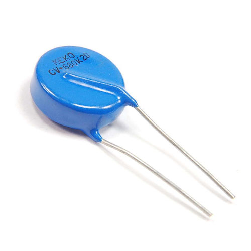
| Definition: A varistor, also known as a voltage-dependent resistor, has an electrical resistance that varies with applied voltage with a nonlinear, non-ohmic current–voltage characteristic, similar to a diode. With low voltage, there is a high electrical resistance which decreases as the voltage is raised, protecting against excessive transient voltages. |
| Definition: A varistor, also known as a voltage-dependent resistor, has an electrical resistance that varies with applied voltage with a nonlinear, non-ohmic current–voltage characteristic, similar to a diode. With low voltage, there is a high electrical resistance which decreases as the voltage is raised, protecting against excessive transient voltages. |
| Definition: A varistor, also known as a voltage-dependent resistor, has an electrical resistance that varies with applied voltage with a nonlinear, non-ohmic current–voltage characteristic, similar to a diode. With low voltage, there is a high electrical resistance which decreases as the voltage is raised, protecting against excessive transient voltages. |
| Definition: A varistor, also known as a voltage-dependent resistor, has an electrical resistance that varies with applied voltage with a nonlinear, non-ohmic current–voltage characteristic, similar to a diode. With low voltage, there is a high electrical resistance which decreases as the voltage is raised, protecting against excessive transient voltages. |
| Definition: A varistor, also known as a voltage-dependent resistor, has an electrical resistance that varies with applied voltage with a nonlinear, non-ohmic current–voltage characteristic, similar to a diode. With low voltage, there is a high electrical resistance which decreases as the voltage is raised, protecting against excessive transient voltages. |
 |
 |
 |
 |
|
|
|
|
|
|
|
|
|
|
|
|
|
|
|
|
| Invented in 1967 by Michio Matsuoka. |
| Invented in 1967 by Michio Matsuoka. |
| Invented in 1967 by Michio Matsuoka. |
| Invented in 1967 by Michio Matsuoka. |
| Invented in 1967 by Michio Matsuoka. |
 |
|
|
|
|
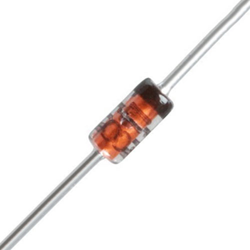
| Definition: Zener diodes provide a stable reference voltage, runs in reverse bias, and breaks down on the arrival of a voltage range and providing a stable voltage. In power supplies, these diodes are widely used to provide a reference voltage. |
| Definition: Zener diodes provide a stable reference voltage, runs in reverse bias, and breaks down on the arrival of a voltage range and providing a stable voltage. In power supplies, these diodes are widely used to provide a reference voltage. |
| Definition: Zener diodes provide a stable reference voltage, runs in reverse bias, and breaks down on the arrival of a voltage range and providing a stable voltage. In power supplies, these diodes are widely used to provide a reference voltage. |
| Definition: Zener diodes provide a stable reference voltage, runs in reverse bias, and breaks down on the arrival of a voltage range and providing a stable voltage. In power supplies, these diodes are widely used to provide a reference voltage. |
| Definition: Zener diodes provide a stable reference voltage, runs in reverse bias, and breaks down on the arrival of a voltage range and providing a stable voltage. In power supplies, these diodes are widely used to provide a reference voltage. |
 |
 |
 |
 |
|
|
|
|
|
|
|
|
|
|
|
|
|
|
|
|
| Invented in 1950 by Clarence Melvin Zener. |
| Invented in 1950 by Clarence Melvin Zener. |
| Invented in 1950 by Clarence Melvin Zener. |
| Invented in 1950 by Clarence Melvin Zener. |
| Invented in 1950 by Clarence Melvin Zener. |
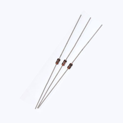
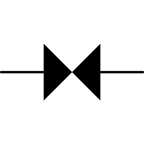
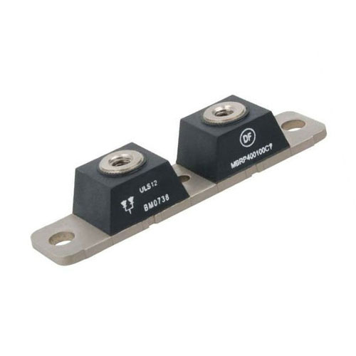
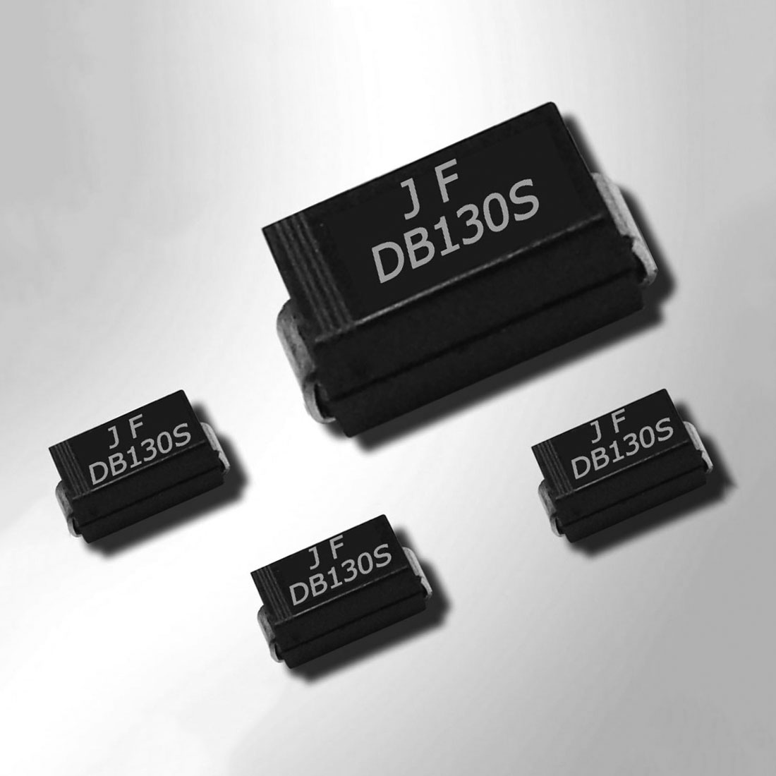
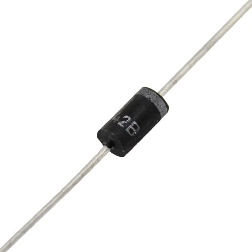
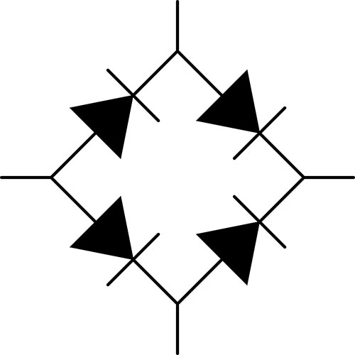
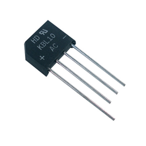
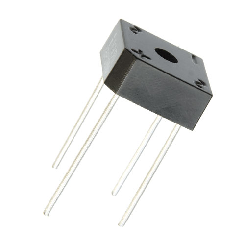
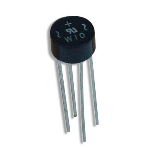
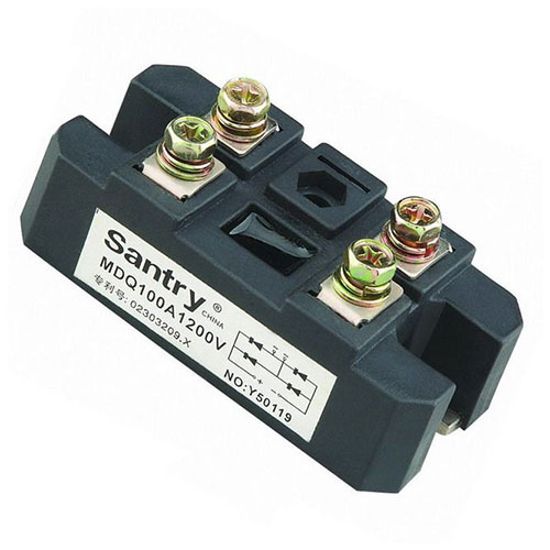
| Rectifier, Full Bridge |
| Rectifier, Full Bridge |
| Rectifier, Full Bridge |
| Rectifier, Full Bridge |
| Rectifier, Full Bridge |
 |
|
|
|
|
| Definition: The conversion of alternating current (AC) input into a direct current (DC) output is known as a full bridge rectifier. This arrangement of four diodes provides the same polarity of output for either polarity of input. |
| Definition: The conversion of alternating current (AC) input into a direct current (DC) output is known as a full bridge rectifier. This arrangement of four diodes provides the same polarity of output for either polarity of input. |
| Definition: The conversion of alternating current (AC) input into a direct current (DC) output is known as a full bridge rectifier. This arrangement of four diodes provides the same polarity of output for either polarity of input. |
| Definition: The conversion of alternating current (AC) input into a direct current (DC) output is known as a full bridge rectifier. This arrangement of four diodes provides the same polarity of output for either polarity of input. |
| Definition: The conversion of alternating current (AC) input into a direct current (DC) output is known as a full bridge rectifier. This arrangement of four diodes provides the same polarity of output for either polarity of input. |
 |
 |
 |
 |
|
|
|
|
|
|
|
|
|
|
|
|
|
|
|
|
| Invented in 1896 by Karol Pollak. |
| Invented in 1896 by Karol Pollak. |
| Invented in 1896 by Karol Pollak. |
| Invented in 1896 by Karol Pollak. |
| Invented in 1896 by Karol Pollak. |
| DIODES · TRANSISTORS INTEGRATED CIRCUITS · THYRISTORS THERMIONIC VALVES |
| DIODES · TRANSISTORS INTEGRATED CIRCUITS · THYRISTORS THERMIONIC VALVES |
| DIODES · TRANSISTORS INTEGRATED CIRCUITS · THYRISTORS THERMIONIC VALVES |
| DIODES · TRANSISTORS INTEGRATED CIRCUITS · THYRISTORS THERMIONIC VALVES |
| DIODES · TRANSISTORS INTEGRATED CIRCUITS · THYRISTORS THERMIONIC VALVES |
| Transistors, an overview |
| Transistors, an overview |
| Transistors, an overview |
| Transistors, an overview |
| Transistors, an overview |
| Includes: Junction, Field Effect and Distinctive Transistors. Definition: Transistors are active components that have at least three electrical contacts and are used in amplifier circuits, switch or logical device. History: In 1907, the first transistor known as the thermionic triode (valve), was used to amplify electronic signals and control electrical power. A solid state version of this device was needed and although some patented the general concept, no working device was made. Not until 1947, when three physicists created the first, solid state point-contact transistor. As the first in a long line of bipolar junction transistors, it is comprised of a germanium crystal in an arrangement with three terminals and two gold point contacts. When connected in a circuit, characteristics illustrated transistor saturation which allowed switching and logic, as an oscillator and when a signal was produced with an output power greater than the input, amplification occurred and their invention would forever change the world landscape of technology. |
| Includes: Junction, Field Effect and Distinctive Transistors. Definition: Transistors are active components that have at least three electrical contacts and are used in amplifier circuits, switch or logical device. History: In 1907, the first transistor known as the thermionic triode (valve), was used to amplify electronic signals and control electrical power. A solid state version of this device was needed and although some patented the general concept, no working device was made. Not until 1947, when three physicists created the first, solid state point-contact transistor. As the first in a long line of bipolar junction transistors, it is comprised of a germanium crystal in an arrangement with three terminals and two gold point contacts. When connected in a circuit, characteristics illustrated transistor saturation which allowed switching and logic, as an oscillator and when a signal was produced with an output power greater than the input, amplification occurred and their invention would forever change the world landscape of technology. |
| Includes: Junction, Field Effect and Distinctive Transistors. Definition: Transistors are active components that have at least three electrical contacts and are used in amplifier circuits, switch or logical device. History: In 1907, the first transistor known as the thermionic triode (valve), was used to amplify electronic signals and control electrical power. A solid state version of this device was needed and although some patented the general concept, no working device was made. Not until 1947, when three physicists created the first, solid state point-contact transistor. As the first in a long line of bipolar junction transistors, it is comprised of a germanium crystal in an arrangement with three terminals and two gold point contacts. When connected in a circuit, characteristics illustrated transistor saturation which allowed switching and logic, as an oscillator and when a signal was produced with an output power greater than the input, amplification occurred and their invention would forever change the world landscape of technology. |
| Includes: Junction, Field Effect and Distinctive Transistors. Definition: Transistors are active components that have at least three electrical contacts and are used in amplifier circuits, switch or logical device. History: In 1907, the first transistor known as the thermionic triode (valve), was used to amplify electronic signals and control electrical power. A solid state version of this device was needed and although some patented the general concept, no working device was made. Not until 1947, when three physicists created the first, solid state point-contact transistor. As the first in a long line of bipolar junction transistors, it is comprised of a germanium crystal in an arrangement with three terminals and two gold point contacts. When connected in a circuit, characteristics illustrated transistor saturation which allowed switching and logic, as an oscillator and when a signal was produced with an output power greater than the input, amplification occurred and their invention would forever change the world landscape of technology. |
| Includes: Junction, Field Effect and Distinctive Transistors. Definition: Transistors are active components that have at least three electrical contacts and are used in amplifier circuits, switch or logical device. History: In 1907, the first transistor known as the thermionic triode (valve), was used to amplify electronic signals and control electrical power. A solid state version of this device was needed and although some patented the general concept, no working device was made. Not until 1947, when three physicists created the first, solid state point-contact transistor. As the first in a long line of bipolar junction transistors, it is comprised of a germanium crystal in an arrangement with three terminals and two gold point contacts. When connected in a circuit, characteristics illustrated transistor saturation which allowed switching and logic, as an oscillator and when a signal was produced with an output power greater than the input, amplification occurred and their invention would forever change the world landscape of technology. |
| Invented in 1907 by John Bardeen. |
| Invented in 1907 by John Bardeen. |
| Invented in 1907 by John Bardeen. |
| Invented in 1907 by John Bardeen. |
| Invented in 1907 by John Bardeen. |
| Transistor, Junction |
| Transistor, Junction |
| Transistor, Junction |
| Transistor, Junction |
| Transistor, Junction |
| Includes: Bipolar Junction, Darlington, Photo and Sziklai Transistors. Members: Alloy Junction, Avalanche, Diffusion, Drift Field, Epitaxial, Grown Junction, Heterojunction Bipolar (HBT), Heterostructure Emitter Bipolar (HEBT), Optical, Pentode, Point Contact, Schottky, Spacistor, Surface Barrier and Tetrode Point Contact Transistors. |
| Includes: Bipolar Junction, Darlington, Photo and Sziklai Transistors. Members: Alloy Junction, Avalanche, Diffusion, Drift Field, Epitaxial, Grown Junction, Heterojunction Bipolar (HBT), Heterostructure Emitter Bipolar (HEBT), Optical, Pentode, Point Contact, Schottky, Spacistor, Surface Barrier and Tetrode Point Contact Transistors. |
| Includes: Bipolar Junction, Darlington, Photo and Sziklai Transistors. Members: Alloy Junction, Avalanche, Diffusion, Drift Field, Epitaxial, Grown Junction, Heterojunction Bipolar (HBT), Heterostructure Emitter Bipolar (HEBT), Optical, Pentode, Point Contact, Schottky, Spacistor, Surface Barrier and Tetrode Point Contact Transistors. |
| Includes: Bipolar Junction, Darlington, Photo and Sziklai Transistors. Members: Alloy Junction, Avalanche, Diffusion, Drift Field, Epitaxial, Grown Junction, Heterojunction Bipolar (HBT), Heterostructure Emitter Bipolar (HEBT), Optical, Pentode, Point Contact, Schottky, Spacistor, Surface Barrier and Tetrode Point Contact Transistors. |
| Includes: Bipolar Junction, Darlington, Photo and Sziklai Transistors. Members: Alloy Junction, Avalanche, Diffusion, Drift Field, Epitaxial, Grown Junction, Heterojunction Bipolar (HBT), Heterostructure Emitter Bipolar (HEBT), Optical, Pentode, Point Contact, Schottky, Spacistor, Surface Barrier and Tetrode Point Contact Transistors. |
|
|
|
|
|
|
|
|
|
|
| Transistor, Bipolar Junction |
| Transistor, Bipolar Junction |
| Transistor, Bipolar Junction |
| Transistor, Bipolar Junction |
| Transistor, Bipolar Junction |
| NPN | PNP |
| NPN | PNP |
| NPN | PNP |
| NPN | PNP |
| NPN | PNP |
| Definition: The Bipolar Junction Transistor (BJT) has two PN junctions, configured as NPN or PNP and are available as individual components, or fabricated within integrated circuits and are utilised as logic, switches or amplifiers. |
| Definition: The Bipolar Junction Transistor (BJT) has two PN junctions, configured as NPN or PNP and are available as individual components, or fabricated within integrated circuits and are utilised as logic, switches or amplifiers. |
| Definition: The Bipolar Junction Transistor (BJT) has two PN junctions, configured as NPN or PNP and are available as individual components, or fabricated within integrated circuits and are utilised as logic, switches or amplifiers. |
| Definition: The Bipolar Junction Transistor (BJT) has two PN junctions, configured as NPN or PNP and are available as individual components, or fabricated within integrated circuits and are utilised as logic, switches or amplifiers. |
| Definition: The Bipolar Junction Transistor (BJT) has two PN junctions, configured as NPN or PNP and are available as individual components, or fabricated within integrated circuits and are utilised as logic, switches or amplifiers. |
| Invented in 1947 by William Bradford Shockley, Walter Brattain & John Bardeen |
| Invented in 1947 by William Bradford Shockley, Walter Brattain & John Bardeen |
| Invented in 1947 by William Bradford Shockley, Walter Brattain & John Bardeen |
| Invented in 1947 by William Bradford Shockley, Walter Brattain & John Bardeen |
| Invented in 1947 by William Bradford Shockley, Walter Brattain & John Bardeen |
| Transistor, Darlington |
| Transistor, Darlington |
| Transistor, Darlington |
| Transistor, Darlington |
| Transistor, Darlington |
| NPN | PNP |
| NPN | PNP |
| NPN | PNP |
| NPN | PNP |
| NPN | PNP |
| Definition: The Darlington Transistor, aka the Darlington Pair, is a bipolar junction transistor that consists of a compound structure with two bipolar transistors arranged in a way, for the current amplified by the first transistor to be further amplified by the second. This results in a current gain that is higher than what could be achieved individually. Integrated Circuit devices benefit from this arrangement of transistors and multiple transistors in an array, by sharing collectors and minimising the number of transistors and the area required for their silicon footprint. |
| Definition: The Darlington Transistor, aka the Darlington Pair, is a bipolar junction transistor that consists of a compound structure with two bipolar transistors arranged in a way, for the current amplified by the first transistor to be further amplified by the second. This results in a current gain that is higher than what could be achieved individually. Integrated Circuit devices benefit from this arrangement of transistors and multiple transistors in an array, by sharing collectors and minimising the number of transistors and the area required for their silicon footprint. |
| Definition: The Darlington Transistor, aka the Darlington Pair, is a bipolar junction transistor that consists of a compound structure with two bipolar transistors arranged in a way, for the current amplified by the first transistor to be further amplified by the second. This results in a current gain that is higher than what could be achieved individually. Integrated Circuit devices benefit from this arrangement of transistors and multiple transistors in an array, by sharing collectors and minimising the number of transistors and the area required for their silicon footprint. |
| Definition: The Darlington Transistor, aka the Darlington Pair, is a bipolar junction transistor that consists of a compound structure with two bipolar transistors arranged in a way, for the current amplified by the first transistor to be further amplified by the second. This results in a current gain that is higher than what could be achieved individually. Integrated Circuit devices benefit from this arrangement of transistors and multiple transistors in an array, by sharing collectors and minimising the number of transistors and the area required for their silicon footprint. |
| Definition: The Darlington Transistor, aka the Darlington Pair, is a bipolar junction transistor that consists of a compound structure with two bipolar transistors arranged in a way, for the current amplified by the first transistor to be further amplified by the second. This results in a current gain that is higher than what could be achieved individually. Integrated Circuit devices benefit from this arrangement of transistors and multiple transistors in an array, by sharing collectors and minimising the number of transistors and the area required for their silicon footprint. |
| Invented in 1953 by Sidney Darlington. |
| Invented in 1953 by Sidney Darlington. |
| Invented in 1953 by Sidney Darlington. |
| Invented in 1953 by Sidney Darlington. |
| Invented in 1953 by Sidney Darlington. |
| NPN | PNP | NPN | PNP |
| NPN | PNP | NPN | PNP |
| NPN | PNP | NPN | PNP |
| NPN | PNP | NPN | PNP |
| NPN | PNP | NPN | PNP |
| Definition: Operated by light rather than electric current, this bipolar transistor is enclosed in a transparent casing to allow light to reach the base collector junction which produce electrons and increase the current gain of the transistor. The phototransistor becomes a photodiode if the emitter is not connected. |
| Definition: Operated by light rather than electric current, this bipolar transistor is enclosed in a transparent casing to allow light to reach the base collector junction which produce electrons and increase the current gain of the transistor. The phototransistor becomes a photodiode if the emitter is not connected. |
| Definition: Operated by light rather than electric current, this bipolar transistor is enclosed in a transparent casing to allow light to reach the base collector junction which produce electrons and increase the current gain of the transistor. The phototransistor becomes a photodiode if the emitter is not connected. |
| Definition: Operated by light rather than electric current, this bipolar transistor is enclosed in a transparent casing to allow light to reach the base collector junction which produce electrons and increase the current gain of the transistor. The phototransistor becomes a photodiode if the emitter is not connected. |
| Definition: Operated by light rather than electric current, this bipolar transistor is enclosed in a transparent casing to allow light to reach the base collector junction which produce electrons and increase the current gain of the transistor. The phototransistor becomes a photodiode if the emitter is not connected. |
| Invented in 1948 by John Northrup Shive. |
| Invented in 1948 by John Northrup Shive. |
| Invented in 1948 by John Northrup Shive. |
| Invented in 1948 by John Northrup Shive. |
| Invented in 1948 by John Northrup Shive. |
| NPN | PNP |
| NPN | PNP |
| NPN | PNP |
| NPN | PNP |
| NPN | PNP |
| Definition: The Sziklai pair, aka the “complementary feedback pair” (CFP), is a configuration of two bipolar transistors, with opposing polarities of NPN and PNP transistors on the same compound transistor. Similar to the Darlington Pair, the Sziklai Pair acts like a single transistor of the same polarity with high current gain and the benefit of a “base turn-on voltage” of 0.6V, half of the nominal turn-on voltage of 1.2V for the Darlington. To improve performance in turn off times and high frequency signals, a resistor of 100Ω to 1kΩ is usually connected between the emitter and base of the transistor with the internal base to collector connection. |
| Definition: The Sziklai pair, aka the “complementary feedback pair” (CFP), is a configuration of two bipolar transistors, with opposing polarities of NPN and PNP transistors on the same compound transistor. Similar to the Darlington Pair, the Sziklai Pair acts like a single transistor of the same polarity with high current gain and the benefit of a “base turn-on voltage” of 0.6V, half of the nominal turn-on voltage of 1.2V for the Darlington. To improve performance in turn off times and high frequency signals, a resistor of 100Ω to 1kΩ is usually connected between the emitter and base of the transistor with the internal base to collector connection. |
| Definition: The Sziklai pair, aka the “complementary feedback pair” (CFP), is a configuration of two bipolar transistors, with opposing polarities of NPN and PNP transistors on the same compound transistor. Similar to the Darlington Pair, the Sziklai Pair acts like a single transistor of the same polarity with high current gain and the benefit of a “base turn-on voltage” of 0.6V, half of the nominal turn-on voltage of 1.2V for the Darlington. To improve performance in turn off times and high frequency signals, a resistor of 100Ω to 1kΩ is usually connected between the emitter and base of the transistor with the internal base to collector connection. |
| Definition: The Sziklai pair, aka the “complementary feedback pair” (CFP), is a configuration of two bipolar transistors, with opposing polarities of NPN and PNP transistors on the same compound transistor. Similar to the Darlington Pair, the Sziklai Pair acts like a single transistor of the same polarity with high current gain and the benefit of a “base turn-on voltage” of 0.6V, half of the nominal turn-on voltage of 1.2V for the Darlington. To improve performance in turn off times and high frequency signals, a resistor of 100Ω to 1kΩ is usually connected between the emitter and base of the transistor with the internal base to collector connection. |
| Definition: The Sziklai pair, aka the “complementary feedback pair” (CFP), is a configuration of two bipolar transistors, with opposing polarities of NPN and PNP transistors on the same compound transistor. Similar to the Darlington Pair, the Sziklai Pair acts like a single transistor of the same polarity with high current gain and the benefit of a “base turn-on voltage” of 0.6V, half of the nominal turn-on voltage of 1.2V for the Darlington. To improve performance in turn off times and high frequency signals, a resistor of 100Ω to 1kΩ is usually connected between the emitter and base of the transistor with the internal base to collector connection. |
| Invented in 1953 by George Clifford Sziklai. |
| Invented in 1953 by George Clifford Sziklai. |
| Invented in 1953 by George Clifford Sziklai. |
| Invented in 1953 by George Clifford Sziklai. |
| Invented in 1953 by George Clifford Sziklai. |
| Transistor, Field Effect |
| Transistor, Field Effect |
| Transistor, Field Effect |
| Transistor, Field Effect |
| Transistor, Field Effect |
| Includes: Junction (JFET) and Insulated Gate (MOSFET), Field Effect Transistors. Members: Ballistic, BIO, CHEMICAL, CNT, DEP, DGMOS, DMOS, DNA, EOS, FIN, FLEX, Floating Gate, FRED, GAA, GNR, HIG, HEMT, IHEMT, IS, IT, JN, LDMOS, MES, MIS, MOD, MUG, Native, NMOS, NOM, O, OTFT, Power, Q, RHBDMOS, SKY, SPIN, SYNAPTIC, T, VES and VMOS FETs. |
| Includes: Junction (JFET) and Insulated Gate (MOSFET), Field Effect Transistors. Members: Ballistic, BIO, CHEMICAL, CNT, DEP, DGMOS, DMOS, DNA, EOS, FIN, FLEX, Floating Gate, FRED, GAA, GNR, HIG, HEMT, IHEMT, IS, IT, JN, LDMOS, MES, MIS, MOD, MUG, Native, NMOS, NOM, O, OTFT, Power, Q, RHBDMOS, SKY, SPIN, SYNAPTIC, T, VES and VMOS FETs. |
| Includes: Junction (JFET) and Insulated Gate (MOSFET), Field Effect Transistors. Members: Ballistic, BIO, CHEMICAL, CNT, DEP, DGMOS, DMOS, DNA, EOS, FIN, FLEX, Floating Gate, FRED, GAA, GNR, HIG, HEMT, IHEMT, IS, IT, JN, LDMOS, MES, MIS, MOD, MUG, Native, NMOS, NOM, O, OTFT, Power, Q, RHBDMOS, SKY, SPIN, SYNAPTIC, T, VES and VMOS FETs. |
| Includes: Junction (JFET) and Insulated Gate (MOSFET), Field Effect Transistors. Members: Ballistic, BIO, CHEMICAL, CNT, DEP, DGMOS, DMOS, DNA, EOS, FIN, FLEX, Floating Gate, FRED, GAA, GNR, HIG, HEMT, IHEMT, IS, IT, JN, LDMOS, MES, MIS, MOD, MUG, Native, NMOS, NOM, O, OTFT, Power, Q, RHBDMOS, SKY, SPIN, SYNAPTIC, T, VES and VMOS FETs. |
| Includes: Junction (JFET) and Insulated Gate (MOSFET), Field Effect Transistors. Members: Ballistic, BIO, CHEMICAL, CNT, DEP, DGMOS, DMOS, DNA, EOS, FIN, FLEX, Floating Gate, FRED, GAA, GNR, HIG, HEMT, IHEMT, IS, IT, JN, LDMOS, MES, MIS, MOD, MUG, Native, NMOS, NOM, O, OTFT, Power, Q, RHBDMOS, SKY, SPIN, SYNAPTIC, T, VES and VMOS FETs. |
| ChN | ChP |
| ChN | ChP |
| ChN | ChP |
| ChN | ChP |
| ChN | ChP |
| Definition: As part of an extensive FET family, the High Electron Mobility Transistor (HEMT), invented in 1979 by Takashi Mimura, is a field effect transistor, in particular, modulation-doped FET (MODFET), which incorporates a junction between two materials, both with different band gaps (heterojunction) as the channel. Aluminium Gallium Arsenide AlGaAs on Gallium Arsenide GaAs or Gallium Nitride GaN on Silicon Carbide have been the 2 material choices and by removing obstacles for the electrons, by creating pathways with the aid of a quantum well, high capacities with low noise is achieved. This translates into millimetre-wave communications with frequencies exceeding 1 THz. Applications for this high speed transistor range from high resolution radar, imaging and radio astronomy to high frequency, band width communication with large compression. |
| Definition: As part of an extensive FET family, the High Electron Mobility Transistor (HEMT), invented in 1979 by Takashi Mimura, is a field effect transistor, in particular, modulation-doped FET (MODFET), which incorporates a junction between two materials, both with different band gaps (heterojunction) as the channel. Aluminium Gallium Arsenide AlGaAs on Gallium Arsenide GaAs or Gallium Nitride GaN on Silicon Carbide have been the 2 material choices and by removing obstacles for the electrons, by creating pathways with the aid of a quantum well, high capacities with low noise is achieved. This translates into millimetre-wave communications with frequencies exceeding 1 THz. Applications for this high speed transistor range from high resolution radar, imaging and radio astronomy to high frequency, band width communication with large compression. |
| Definition: As part of an extensive FET family, the High Electron Mobility Transistor (HEMT), invented in 1979 by Takashi Mimura, is a field effect transistor, in particular, modulation-doped FET (MODFET), which incorporates a junction between two materials, both with different band gaps (heterojunction) as the channel. Aluminium Gallium Arsenide AlGaAs on Gallium Arsenide GaAs or Gallium Nitride GaN on Silicon Carbide have been the 2 material choices and by removing obstacles for the electrons, by creating pathways with the aid of a quantum well, high capacities with low noise is achieved. This translates into millimetre-wave communications with frequencies exceeding 1 THz. Applications for this high speed transistor range from high resolution radar, imaging and radio astronomy to high frequency, band width communication with large compression. |
| Definition: As part of an extensive FET family, the High Electron Mobility Transistor (HEMT), invented in 1979 by Takashi Mimura, is a field effect transistor, in particular, modulation-doped FET (MODFET), which incorporates a junction between two materials, both with different band gaps (heterojunction) as the channel. Aluminium Gallium Arsenide AlGaAs on Gallium Arsenide GaAs or Gallium Nitride GaN on Silicon Carbide have been the 2 material choices and by removing obstacles for the electrons, by creating pathways with the aid of a quantum well, high capacities with low noise is achieved. This translates into millimetre-wave communications with frequencies exceeding 1 THz. Applications for this high speed transistor range from high resolution radar, imaging and radio astronomy to high frequency, band width communication with large compression. |
| Definition: As part of an extensive FET family, the High Electron Mobility Transistor (HEMT), invented in 1979 by Takashi Mimura, is a field effect transistor, in particular, modulation-doped FET (MODFET), which incorporates a junction between two materials, both with different band gaps (heterojunction) as the channel. Aluminium Gallium Arsenide AlGaAs on Gallium Arsenide GaAs or Gallium Nitride GaN on Silicon Carbide have been the 2 material choices and by removing obstacles for the electrons, by creating pathways with the aid of a quantum well, high capacities with low noise is achieved. This translates into millimetre-wave communications with frequencies exceeding 1 THz. Applications for this high speed transistor range from high resolution radar, imaging and radio astronomy to high frequency, band width communication with large compression. |
| Invented in 1925 by Julius Edgar Lilienfeld. |
| Invented in 1925 by Julius Edgar Lilienfeld. |
| Invented in 1925 by Julius Edgar Lilienfeld. |
| Invented in 1925 by Julius Edgar Lilienfeld. |
| Invented in 1925 by Julius Edgar Lilienfeld. |
| DM-ChN | DM-ChP | EM-ChN | EM-ChP |
| DM-ChN | DM-ChP | EM-ChN | EM-ChP |
| DM-ChN | DM-ChP | EM-ChN | EM-ChP |
| DM-ChN | DM-ChP | EM-ChN | EM-ChP |
| DM-ChN | DM-ChP | EM-ChN | EM-ChP |
| G2-DM-ChN | G2-DM-ChP | G2-EM-ChN | G2-EM-ChP |
| G2-DM-ChN | G2-DM-ChP | G2-EM-ChN | G2-EM-ChP |
| G2-DM-ChN | G2-DM-ChP | G2-EM-ChN | G2-EM-ChP |
| G2-DM-ChN | G2-DM-ChP | G2-EM-ChN | G2-EM-ChP |
| G2-DM-ChN | G2-DM-ChP | G2-EM-ChN | G2-EM-ChP |
| PWR-DM-ChN | PWR-DM-ChP | PWR-EM-ChN | PWR-EM-ChP |
| PWR-DM-ChN | PWR-DM-ChP | PWR-EM-ChN | PWR-EM-ChP |
| PWR-DM-ChN | PWR-DM-ChP | PWR-EM-ChN | PWR-EM-ChP |
| PWR-DM-ChN | PWR-DM-ChP | PWR-EM-ChN | PWR-EM-ChP |
| PWR-DM-ChN | PWR-DM-ChP | PWR-EM-ChN | PWR-EM-ChP |
| PWR-G2-DM-ChN | PWR-G2-DM-ChP | PWR-G2-EM-ChN | PWR-G2-EM-ChP |
| PWR-G2-DM-ChN | PWR-G2-DM-ChP | PWR-G2-EM-ChN | PWR-G2-EM-ChP |
| PWR-G2-DM-ChN | PWR-G2-DM-ChP | PWR-G2-EM-ChN | PWR-G2-EM-ChP |
| PWR-G2-DM ChN |
PWR-G2-DM ChP |
PWR-G2-EM ChN |
PWR-G2-EM ChP |
| PWR-G2-DM ChN |
PWR-G2-DM ChP |
PWR-G2-EM ChN |
PWR-G2-EM ChP |
| MOSFET = Metal Oxide Semiconductor Field Effect Transistor ChN = Negative Channel · ChP = Positive Channel DM = Depleted Mode · EM = Enhanced Mode PWR = Power · G2 = 2 Gates |
| MOSFET = Metal Oxide Semiconductor Field Effect Transistor ChN = Negative Channel · ChP = Positive Channel DM = Depleted Mode · EM = Enhanced Mode PWR = Power · G2 = 2 Gates |
| MOSFET = Metal Oxide Semiconductor Field Effect Transistor ChN = Negative Channel · ChP = Positive Channel DM = Depleted Mode · EM = Enhanced Mode PWR = Power · G2 = 2 Gates |
| MOSFET Metal Oxide Semiconductor Field Effect Transistor ChN Negative Channel · ChP Positive Channel DM Depleted Mode · EM Enhanced Mode PWR Power · G2 2 Gates |
| MOSFET Metal Oxide Semiconductor Field Effect Transistor ChN Negative Channel · ChP Positive Channel DM Depleted Mode · EM Enhanced Mode PWR Power · G2 2 Gates |
| Transistor, Distinctive |
| Transistor, Distinctive |
| Transistor, Distinctive |
| Transistor, Distinctive |
| Transistor, Distinctive |
| Includes: IGBT and Unijunction Transistors. Members: Multiple Emitter and Collector Emitter Transistors. |
| Includes: IGBT and Unijunction Transistors. Members: Multiple Emitter and Collector Emitter Transistors. |
| Includes: IGBT and Unijunction Transistors. Members: Multiple Emitter and Collector Emitter Transistors. |
| Includes: IGBT and Unijunction Transistors. Members: Multiple Emitter and Collector Emitter Transistors. |
| Includes: IGBT and Unijunction Transistors. Members: Multiple Emitter and Collector Emitter Transistors. |
|
|
|
|
|
|
|
|
|
|
| D-ChN | D-ChP | E-ChN | E-ChP |
| D-ChN | D-ChP | E-ChN | E-ChP |
| D-ChN | D-ChP | E-ChN | E-ChP |
| D-ChN | D-ChP | E-ChN | E-ChP |
| D-ChN | D-ChP | E-ChN | E-ChP |
| Definition: The Insulated Gate Bipolar Transistor (IGBT), is a hybrid of a Bipolar Junction Transistor and a Field Effect Transistor, forming an exceptional semiconductor switching device. High input impedance and high switching speeds of a MOSFET with low saturation voltage of a bipolar transistor, creates a switching device that can handle large collector-emitter currents. These transistors are used in inverters, converters and power supplies. The advantage gained of the IGBT over the BJT or MOSFET, is the greater power gain than the bipolar junction type transistor and the higher voltage operation with low input losses of the MOSFET. |
| Definition: The Insulated Gate Bipolar Transistor (IGBT), is a hybrid of a Bipolar Junction Transistor and a Field Effect Transistor, forming an exceptional semiconductor switching device. High input impedance and high switching speeds of a MOSFET with low saturation voltage of a bipolar transistor, creates a switching device that can handle large collector-emitter currents. These transistors are used in inverters, converters and power supplies. The advantage gained of the IGBT over the BJT or MOSFET, is the greater power gain than the bipolar junction type transistor and the higher voltage operation with low input losses of the MOSFET. |
| Definition: The Insulated Gate Bipolar Transistor (IGBT), is a hybrid of a Bipolar Junction Transistor and a Field Effect Transistor, forming an exceptional semiconductor switching device. High input impedance and high switching speeds of a MOSFET with low saturation voltage of a bipolar transistor, creates a switching device that can handle large collector-emitter currents. These transistors are used in inverters, converters and power supplies. The advantage gained of the IGBT over the BJT or MOSFET, is the greater power gain than the bipolar junction type transistor and the higher voltage operation with low input losses of the MOSFET. |
| Definition: The Insulated Gate Bipolar Transistor (IGBT), is a hybrid of a Bipolar Junction Transistor and a Field Effect Transistor, forming an exceptional semiconductor switching device. High input impedance and high switching speeds of a MOSFET with low saturation voltage of a bipolar transistor, creates a switching device that can handle large collector-emitter currents. These transistors are used in inverters, converters and power supplies. The advantage gained of the IGBT over the BJT or MOSFET, is the greater power gain than the bipolar junction type transistor and the higher voltage operation with low input losses of the MOSFET. |
| Definition: The Insulated Gate Bipolar Transistor (IGBT), is a hybrid of a Bipolar Junction Transistor and a Field Effect Transistor, forming an exceptional semiconductor switching device. High input impedance and high switching speeds of a MOSFET with low saturation voltage of a bipolar transistor, creates a switching device that can handle large collector-emitter currents. These transistors are used in inverters, converters and power supplies. The advantage gained of the IGBT over the BJT or MOSFET, is the greater power gain than the bipolar junction type transistor and the higher voltage operation with low input losses of the MOSFET. |
| Invented in 1982 by Jayant Baliga. |
| Invented in 1982 by Jayant Baliga. |
| Invented in 1982 by Jayant Baliga. |
| Invented in 1982 by Jayant Baliga. |
| Invented in 1982 by Jayant Baliga. |
| Transistor, Unijunction |
| Transistor, Unijunction |
| Transistor, Unijunction |
| Transistor, Unijunction |
| Transistor, Unijunction |
| ChN | ChP |
| ChN | ChP |
| ChN | ChP |
| ChN | ChP |
| ChN | ChP |
| Definition: Unijunction Transistor (UJT) aka the double base diode, was invented by accident while working evaluating experimental tetrode transistors. The tetrodes, made by Arnold Lesk, showed a hysteresis effect on the input and discovered on the oscilloscope that the device was oscillating. The collector was disconnected and the test transistors were enclosed in glass vials filled with silicone oil, with the leads sealed with wax. By accident, an active device consisting of an emitter-base junction and two ohmic connections to the base had been made. It had negative resistance and could be made to oscillate and act as a trigger. The silicon version of the unijunction transistors (2N489-2N494) were made and used in circuits for SCR triggering. |
| Definition: Unijunction Transistor (UJT) aka the double base diode, was invented by accident while working evaluating experimental tetrode transistors. The tetrodes, made by Arnold Lesk, showed a hysteresis effect on the input and discovered on the oscilloscope that the device was oscillating. The collector was disconnected and the test transistors were enclosed in glass vials filled with silicone oil, with the leads sealed with wax. By accident, an active device consisting of an emitter-base junction and two ohmic connections to the base had been made. It had negative resistance and could be made to oscillate and act as a trigger. The silicon version of the unijunction transistors (2N489-2N494) were made and used in circuits for SCR triggering. |
| Definition: Unijunction Transistor (UJT) aka the double base diode, was invented by accident while working evaluating experimental tetrode transistors. The tetrodes, made by Arnold Lesk, showed a hysteresis effect on the input and discovered on the oscilloscope that the device was oscillating. The collector was disconnected and the test transistors were enclosed in glass vials filled with silicone oil, with the leads sealed with wax. By accident, an active device consisting of an emitter-base junction and two ohmic connections to the base had been made. It had negative resistance and could be made to oscillate and act as a trigger. The silicon version of the unijunction transistors (2N489-2N494) were made and used in circuits for SCR triggering. |
| Definition: Unijunction Transistor (UJT) aka the double base diode, was invented by accident while working evaluating experimental tetrode transistors. The tetrodes, made by Arnold Lesk, showed a hysteresis effect on the input and discovered on the oscilloscope that the device was oscillating. The collector was disconnected and the test transistors were enclosed in glass vials filled with silicone oil, with the leads sealed with wax. By accident, an active device consisting of an emitter-base junction and two ohmic connections to the base had been made. It had negative resistance and could be made to oscillate and act as a trigger. The silicon version of the unijunction transistors (2N489-2N494) were made and used in circuits for SCR triggering. |
| Definition: Unijunction Transistor (UJT) aka the double base diode, was invented by accident while working evaluating experimental tetrode transistors. The tetrodes, made by Arnold Lesk, showed a hysteresis effect on the input and discovered on the oscilloscope that the device was oscillating. The collector was disconnected and the test transistors were enclosed in glass vials filled with silicone oil, with the leads sealed with wax. By accident, an active device consisting of an emitter-base junction and two ohmic connections to the base had been made. It had negative resistance and could be made to oscillate and act as a trigger. The silicon version of the unijunction transistors (2N489-2N494) were made and used in circuits for SCR triggering. |
| Invented in 1953 by Arnold Lesk. |
| Invented in 1953 by Arnold Lesk. |
| Invented in 1953 by Arnold Lesk. |
| Invented in 1953 by Arnold Lesk. |
| Invented in 1953 by Arnold Lesk. |
| DIODES · TRANSISTORS INTEGRATED CIRCUITS · THYRISTORS THERMIONIC VALVES |
| DIODES · TRANSISTORS INTEGRATED CIRCUITS · THYRISTORS THERMIONIC VALVES |
| DIODES · TRANSISTORS INTEGRATED CIRCUITS · THYRISTORS THERMIONIC VALVES |
| DIODES · TRANSISTORS INTEGRATED CIRCUITS · THYRISTORS THERMIONIC VALVES |
| DIODES · TRANSISTORS INTEGRATED CIRCUITS · THYRISTORS THERMIONIC VALVES |
| Integrated Circuits, an overview |
| Integrated Circuits, an overview |
| Integrated Circuits, an overview |
| Integrated Circuits, an overview |
| Integrated Circuits, an overview |
| Definition: ICs, chips, or microchips and are a combined set of electronic circuits on one small plate (chip) of silicon. Within 1 square centimetre, billions of transistors with a countless array of diverse components are combined to achieve functions of processing, storage and IO control. Currently, transistors are at a width of 14 nanometres with a view to reduce to 5 nanometres by 2020. In 1953, the first transistor computer, had 92 point-contact transistors at a width of 12.5mm. In 1971, the first microprocessor on a single integrated circuit (TMS1000) had 8,000 transistors at a width of 8 micrometres. In 2015, a microprocessor on a single integrated circuit (Intel) has well over 5 billion transistors at a width of 15 nanometres. DIP, Dual Inline Package, refers to the packaging of an integrated circuit with a ceramic body and two rows of pins standardised in 1965 by Electrical Engineer, Bryant (Buck) Rogers. The spacing between the rows (the width) and the distance between the pins (the pitch) are defined by industry standards in pin counts of 4, 6, 8, 14, 16, 18, 20, 22, 24, 28, 32, 40, and 64. |
| Definition: ICs, chips, or microchips and are a combined set of electronic circuits on one small plate (chip) of silicon. Within 1 square centimetre, billions of transistors with a countless array of diverse components are combined to achieve functions of processing, storage and IO control. Currently, transistors are at a width of 14 nanometres with a view to reduce to 5 nanometres by 2020. In 1953, the first transistor computer, had 92 point-contact transistors at a width of 12.5mm. In 1971, the first microprocessor on a single integrated circuit (TMS1000) had 8,000 transistors at a width of 8 micrometres. In 2015, a microprocessor on a single integrated circuit (Intel) has well over 5 billion transistors at a width of 15 nanometres. DIP, Dual Inline Package, refers to the packaging of an integrated circuit with a ceramic body and two rows of pins standardised in 1965 by Electrical Engineer, Bryant (Buck) Rogers. The spacing between the rows (the width) and the distance between the pins (the pitch) are defined by industry standards in pin counts of 4, 6, 8, 14, 16, 18, 20, 22, 24, 28, 32, 40, and 64. |
| Definition: ICs, chips, or microchips and are a combined set of electronic circuits on one small plate (chip) of silicon. Within 1 square centimetre, billions of transistors with a countless array of diverse components are combined to achieve functions of processing, storage and IO control. Currently, transistors are at a width of 14 nanometres with a view to reduce to 5 nanometres by 2020. In 1953, the first transistor computer, had 92 point-contact transistors at a width of 12.5mm. In 1971, the first microprocessor on a single integrated circuit (TMS1000) had 8,000 transistors at a width of 8 micrometres. In 2015, a microprocessor on a single integrated circuit (Intel) has well over 5 billion transistors at a width of 15 nanometres. DIP, Dual Inline Package, refers to the packaging of an integrated circuit with a ceramic body and two rows of pins standardised in 1965 by Electrical Engineer, Bryant (Buck) Rogers. The spacing between the rows (the width) and the distance between the pins (the pitch) are defined by industry standards in pin counts of 4, 6, 8, 14, 16, 18, 20, 22, 24, 28, 32, 40, and 64. |
| Definition: ICs, chips, or microchips and are a combined set of electronic circuits on one small plate (chip) of silicon. Within 1 square centimetre, billions of transistors with a countless array of diverse components are combined to achieve functions of processing, storage and IO control. Currently, transistors are at a width of 14 nanometres with a view to reduce to 5 nanometres by 2020. In 1953, the first transistor computer, had 92 point-contact transistors at a width of 12.5mm. In 1971, the first microprocessor on a single integrated circuit (TMS1000) had 8,000 transistors at a width of 8 micrometres. In 2015, a microprocessor on a single integrated circuit (Intel) has well over 5 billion transistors at a width of 15 nanometres. DIP, Dual Inline Package, refers to the packaging of an integrated circuit with a ceramic body and two rows of pins standardised in 1965 by Electrical Engineer, Bryant (Buck) Rogers. The spacing between the rows (the width) and the distance between the pins (the pitch) are defined by industry standards in pin counts of 4, 6, 8, 14, 16, 18, 20, 22, 24, 28, 32, 40, and 64. |
| Definition: ICs, chips, or microchips and are a combined set of electronic circuits on one small plate (chip) of silicon. Within 1 square centimetre, billions of transistors with a countless array of diverse components are combined to achieve functions of processing, storage and IO control. Currently, transistors are at a width of 14 nanometres with a view to reduce to 5 nanometres by 2020. In 1953, the first transistor computer, had 92 point-contact transistors at a width of 12.5mm. In 1971, the first microprocessor on a single integrated circuit (TMS1000) had 8,000 transistors at a width of 8 micrometres. In 2015, a microprocessor on a single integrated circuit (Intel) has well over 5 billion transistors at a width of 15 nanometres. DIP, Dual Inline Package, refers to the packaging of an integrated circuit with a ceramic body and two rows of pins standardised in 1965 by Electrical Engineer, Bryant (Buck) Rogers. The spacing between the rows (the width) and the distance between the pins (the pitch) are defined by industry standards in pin counts of 4, 6, 8, 14, 16, 18, 20, 22, 24, 28, 32, 40, and 64. |
 |
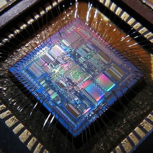 |
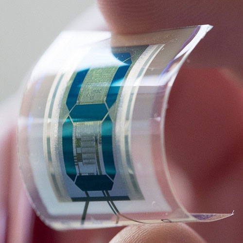 |
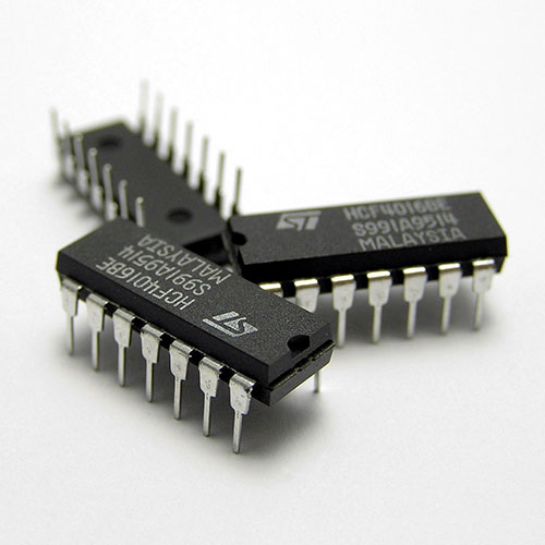 |
|
|
|
|
|
|
|
|
|
|
|
|
|
|
|
|
| Invented in 1958 by Jack Kilby. |
| Invented in 1958 by Jack Kilby. |
| Invented in 1958 by Jack Kilby. |
| Invented in 1958 by Jack Kilby. |
| Invented in 1958 by Jack Kilby. |
| DIODES · TRANSISTORS INTEGRATED CIRCUITS · THYRISTORS THERMIONIC VALVES |
| DIODES · TRANSISTORS INTEGRATED CIRCUITS · THYRISTORS THERMIONIC VALVES |
| DIODES · TRANSISTORS INTEGRATED CIRCUITS · THYRISTORS THERMIONIC VALVES |
| DIODES · TRANSISTORS INTEGRATED CIRCUITS · THYRISTORS THERMIONIC VALVES |
| DIODES · TRANSISTORS INTEGRATED CIRCUITS · THYRISTORS THERMIONIC VALVES |
| Thyristors, an overview |
| Thyristors, an overview |
| Thyristors, an overview |
| Thyristors, an overview |
| Thyristors, an overview |
| Includes: Darlistor, Photo, Quadrac, SBS, SCR, SCS, SUS and Triac Thyristors. Members: ACS, ACST, AGT, ASCR, BCT, BOD, Dynistor, Trisil, SIDACtor, BRT, ETO, GTO, MA-GTO, IGCT, LASCR, MCT, CSMT, PUT, RCT and SITh Thyristors. Definition: Thyristors were developed as a solid state replacement for mechanical relays with high “off” impedance and were based on silicon with four alternating layers of N and P-type material. The Anode terminal connects to the first P Layer, N layer, then the Gate terminal at the second P layer, then the final N layer connects to the Cathode terminal (Anode – P, N, Gate – P, N – Cathode). By applying a trigger voltage to the Gate terminal, the thyristor will conduct, acting as a bistable switch until the forward current drops below the threshold value (holding current) or the voltage across the device is not reversed (forward-biased). |
| Includes: Darlistor, Photo, Quadrac, SBS, SCR, SCS, SUS and Triac Thyristors. Members: ACS, ACST, AGT, ASCR, BCT, BOD, Dynistor, Trisil, SIDACtor, BRT, ETO, GTO, MA-GTO, IGCT, LASCR, MCT, CSMT, PUT, RCT and SITh Thyristors. Definition: Thyristors were developed as a solid state replacement for mechanical relays with high “off” impedance and were based on silicon with four alternating layers of N and P-type material. The Anode terminal connects to the first P Layer, N layer, then the Gate terminal at the second P layer, then the final N layer connects to the Cathode terminal (Anode – P, N, Gate – P, N – Cathode). By applying a trigger voltage to the Gate terminal, the thyristor will conduct, acting as a bistable switch until the forward current drops below the threshold value (holding current) or the voltage across the device is not reversed (forward-biased). |
| Includes: Darlistor, Photo, Quadrac, SBS, SCR, SCS, SUS and Triac Thyristors. Members: ACS, ACST, AGT, ASCR, BCT, BOD, Dynistor, Trisil, SIDACtor, BRT, ETO, GTO, MA-GTO, IGCT, LASCR, MCT, CSMT, PUT, RCT and SITh Thyristors. Definition: Thyristors were developed as a solid state replacement for mechanical relays with high “off” impedance and were based on silicon with four alternating layers of N and P-type material. The Anode terminal connects to the first P Layer, N layer, then the Gate terminal at the second P layer, then the final N layer connects to the Cathode terminal (Anode – P, N, Gate – P, N – Cathode). By applying a trigger voltage to the Gate terminal, the thyristor will conduct, acting as a bistable switch until the forward current drops below the threshold value (holding current) or the voltage across the device is not reversed (forward-biased). |
| Includes: Darlistor, Photo, Quadrac, SBS, SCR, SCS, SUS and Triac Thyristors. Members: ACS, ACST, AGT, ASCR, BCT, BOD, Dynistor, Trisil, SIDACtor, BRT, ETO, GTO, MA-GTO, IGCT, LASCR, MCT, CSMT, PUT, RCT and SITh Thyristors. Definition: Thyristors were developed as a solid state replacement for mechanical relays with high “off” impedance and were based on silicon with four alternating layers of N and P-type material. The Anode terminal connects to the first P Layer, N layer, then the Gate terminal at the second P layer, then the final N layer connects to the Cathode terminal (Anode – P, N, Gate – P, N – Cathode). By applying a trigger voltage to the Gate terminal, the thyristor will conduct, acting as a bistable switch until the forward current drops below the threshold value (holding current) or the voltage across the device is not reversed (forward-biased). |
| Includes: Darlistor, Photo, Quadrac, SBS, SCR, SCS, SUS and Triac Thyristors. Members: ACS, ACST, AGT, ASCR, BCT, BOD, Dynistor, Trisil, SIDACtor, BRT, ETO, GTO, MA-GTO, IGCT, LASCR, MCT, CSMT, PUT, RCT and SITh Thyristors. Definition: Thyristors were developed as a solid state replacement for mechanical relays with high “off” impedance and were based on silicon with four alternating layers of N and P-type material. The Anode terminal connects to the first P Layer, N layer, then the Gate terminal at the second P layer, then the final N layer connects to the Cathode terminal (Anode – P, N, Gate – P, N – Cathode). By applying a trigger voltage to the Gate terminal, the thyristor will conduct, acting as a bistable switch until the forward current drops below the threshold value (holding current) or the voltage across the device is not reversed (forward-biased). |
| Invented in 1957 by William (Bill) Gutzwiller & Gordon Hall. |
| Invented in 1957 by William (Bill) Gutzwiller & Gordon Hall. |
| Invented in 1957 by William (Bill) Gutzwiller & Gordon Hall. |
| Invented in 1957 by William (Bill) Gutzwiller & Gordon Hall. |
| Invented in 1957 by William (Bill) Gutzwiller & Gordon Hall. |
| Thyristor, Darlistor |
| Thyristor, Darlistor |
| Thyristor, Darlistor |
| Thyristor, Darlistor |
| Thyristor, Darlistor |
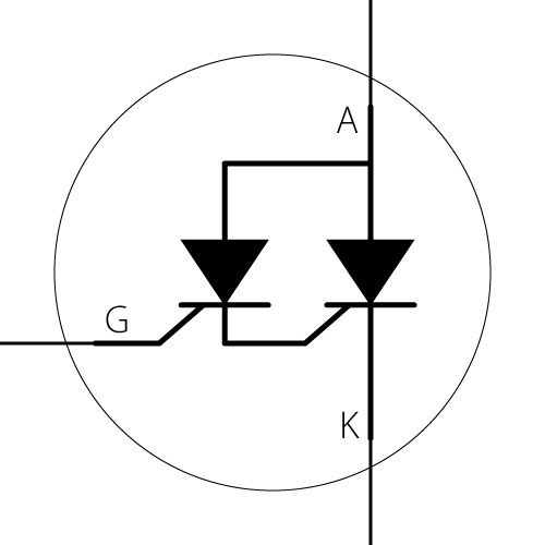 |
|
|
|
|
| Definition: Compound thyristor, similar in composition and operation, to a darlington pair of transistors, that is an internally amplifying and fast switching. They comprise of a vertical thyristor with a localised anode region and a cathode coating the rear region, with a lateral thyristor on the front region. The thyristor gate corresponds to the cathode-gate region of the lateral thyristor with the cathode-gate of the lateral thyristor connected to the cathode of the vertical thyristor. |
| Definition: Compound thyristor, similar in composition and operation, to a darlington pair of transistors, that is an internally amplifying and fast switching. They comprise of a vertical thyristor with a localised anode region and a cathode coating the rear region, with a lateral thyristor on the front region. The thyristor gate corresponds to the cathode-gate region of the lateral thyristor with the cathode-gate of the lateral thyristor connected to the cathode of the vertical thyristor. |
| Definition: Compound thyristor, similar in composition and operation, to a darlington pair of transistors, that is an internally amplifying and fast switching. They comprise of a vertical thyristor with a localised anode region and a cathode coating the rear region, with a lateral thyristor on the front region. The thyristor gate corresponds to the cathode-gate region of the lateral thyristor with the cathode-gate of the lateral thyristor connected to the cathode of the vertical thyristor. |
| Definition: Compound thyristor, similar in composition and operation, to a darlington pair of transistors, that is an internally amplifying and fast switching. They comprise of a vertical thyristor with a localised anode region and a cathode coating the rear region, with a lateral thyristor on the front region. The thyristor gate corresponds to the cathode-gate region of the lateral thyristor with the cathode-gate of the lateral thyristor connected to the cathode of the vertical thyristor. |
| Definition: Compound thyristor, similar in composition and operation, to a darlington pair of transistors, that is an internally amplifying and fast switching. They comprise of a vertical thyristor with a localised anode region and a cathode coating the rear region, with a lateral thyristor on the front region. The thyristor gate corresponds to the cathode-gate region of the lateral thyristor with the cathode-gate of the lateral thyristor connected to the cathode of the vertical thyristor. |
| Invented in 1971 by Robert Pezzani. |
| Invented in 1971 by Robert Pezzani. |
| Invented in 1971 by Robert Pezzani. |
| Invented in 1971 by Robert Pezzani. |
| Invented in 1971 by Robert Pezzani. |
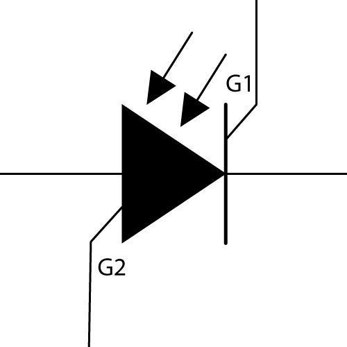 |
|
|
|
|
| Definition: Monolithic semiconductor switch which is triggering from a light source to a light sensitive gate region or to an amplified gate thyristor region, connected to an electrical triggering source. Photothyristors are insensitive to electrical signals, encouraging use within electrically noisy environments. Light-triggered thyristors are an advantage in high-voltage applications as they are in-built with over-voltage (VBO) protection. There are 2 main photothyristors, the light-activated SCR (LASCR) and the light-activated TRIAC. |
| Definition: Monolithic semiconductor switch which is triggering from a light source to a light sensitive gate region or to an amplified gate thyristor region, connected to an electrical triggering source. Photothyristors are insensitive to electrical signals, encouraging use within electrically noisy environments. Light-triggered thyristors are an advantage in high-voltage applications as they are in-built with over-voltage (VBO) protection. There are 2 main photothyristors, the light-activated SCR (LASCR) and the light-activated TRIAC. |
| Definition: Monolithic semiconductor switch which is triggering from a light source to a light sensitive gate region or to an amplified gate thyristor region, connected to an electrical triggering source. Photothyristors are insensitive to electrical signals, encouraging use within electrically noisy environments. Light-triggered thyristors are an advantage in high-voltage applications as they are in-built with over-voltage (VBO) protection. There are 2 main photothyristors, the light-activated SCR (LASCR) and the light-activated TRIAC. |
| Definition: Monolithic semiconductor switch which is triggering from a light source to a light sensitive gate region or to an amplified gate thyristor region, connected to an electrical triggering source. Photothyristors are insensitive to electrical signals, encouraging use within electrically noisy environments. Light-triggered thyristors are an advantage in high-voltage applications as they are in-built with over-voltage (VBO) protection. There are 2 main photothyristors, the light-activated SCR (LASCR) and the light-activated TRIAC. |
| Definition: Monolithic semiconductor switch which is triggering from a light source to a light sensitive gate region or to an amplified gate thyristor region, connected to an electrical triggering source. Photothyristors are insensitive to electrical signals, encouraging use within electrically noisy environments. Light-triggered thyristors are an advantage in high-voltage applications as they are in-built with over-voltage (VBO) protection. There are 2 main photothyristors, the light-activated SCR (LASCR) and the light-activated TRIAC. |
| Invented in 1975 by Herbert F Storm. |
| Invented in 1975 by Herbert F Storm. |
| Invented in 1975 by Herbert F Storm. |
| Invented in 1975 by Herbert F Storm. |
| Invented in 1975 by Herbert F Storm. |
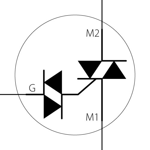 |
|
|
|
|
| Definition: The Quadrac is a compound special type of thyristor which combines a “diac (trigger for the triac)” and a “triac (solid state AC relay)” as one component with the benefits of matching specifications and rating the pair. When triggered, thyristors turn on to provide low-resistance paths for current and remain so until the current is reduced to a specific level, triggered off or switched off. This invention was established at the inception of the thyristor, more specifically, the silicone controlled rectifier (SCR). Quadracs are commonly used to control lighting, speed and temperature. Key specifications of peak repetitive off voltage, peak repetitive reverse voltage, root mean square (RMS) on-state current and temperature junction. |
| Definition: The Quadrac is a compound special type of thyristor which combines a “diac (trigger for the triac)” and a “triac (solid state AC relay)” as one component with the benefits of matching specifications and rating the pair. When triggered, thyristors turn on to provide low-resistance paths for current and remain so until the current is reduced to a specific level, triggered off or switched off. This invention was established at the inception of the thyristor, more specifically, the silicone controlled rectifier (SCR). Quadracs are commonly used to control lighting, speed and temperature. Key specifications of peak repetitive off voltage, peak repetitive reverse voltage, root mean square (RMS) on-state current and temperature junction. |
| Definition: The Quadrac is a compound special type of thyristor which combines a “diac (trigger for the triac)” and a “triac (solid state AC relay)” as one component with the benefits of matching specifications and rating the pair. When triggered, thyristors turn on to provide low-resistance paths for current and remain so until the current is reduced to a specific level, triggered off or switched off. This invention was established at the inception of the thyristor, more specifically, the silicone controlled rectifier (SCR). Quadracs are commonly used to control lighting, speed and temperature. Key specifications of peak repetitive off voltage, peak repetitive reverse voltage, root mean square (RMS) on-state current and temperature junction. |
| Definition: The Quadrac is a compound special type of thyristor which combines a “diac (trigger for the triac)” and a “triac (solid state AC relay)” as one component with the benefits of matching specifications and rating the pair. When triggered, thyristors turn on to provide low-resistance paths for current and remain so until the current is reduced to a specific level, triggered off or switched off. This invention was established at the inception of the thyristor, more specifically, the silicone controlled rectifier (SCR). Quadracs are commonly used to control lighting, speed and temperature. Key specifications of peak repetitive off voltage, peak repetitive reverse voltage, root mean square (RMS) on-state current and temperature junction. |
| Definition: The Quadrac is a compound special type of thyristor which combines a “diac (trigger for the triac)” and a “triac (solid state AC relay)” as one component with the benefits of matching specifications and rating the pair. When triggered, thyristors turn on to provide low-resistance paths for current and remain so until the current is reduced to a specific level, triggered off or switched off. This invention was established at the inception of the thyristor, more specifically, the silicone controlled rectifier (SCR). Quadracs are commonly used to control lighting, speed and temperature. Key specifications of peak repetitive off voltage, peak repetitive reverse voltage, root mean square (RMS) on-state current and temperature junction. |
| Invented in 1957 by William (Bill) Gutzwiller & Gordon Hall. |
| Invented in 1957 by William (Bill) Gutzwiller & Gordon Hall. |
| Invented in 1957 by William (Bill) Gutzwiller & Gordon Hall. |
| Invented in 1957 by William (Bill) Gutzwiller & Gordon Hall. |
| Invented in 1957 by William (Bill) Gutzwiller & Gordon Hall. |
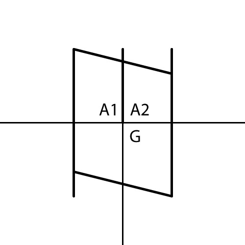 |
|
|
|
|
| Definition: Device capable of triggering triacs and lower breakover voltage than a diac, with ± 8 V being the preferred rating. The SBS and the diac have a similar V-I characteristic curve, however, it has a more pronounced “negative resistance” region and when switching to a conducting state the voltage drops below 1 volt. The modern SBS has a stable temperature coefficient of + 0.02 % per °C, with a VB0 increase of 0.02 % per degree of rising temperature (0.16 V per 100°C). |
| Definition: Device capable of triggering triacs and lower breakover voltage than a diac, with ± 8 V being the preferred rating. The SBS and the diac have a similar V-I characteristic curve, however, it has a more pronounced “negative resistance” region and when switching to a conducting state the voltage drops below 1 volt. The modern SBS has a stable temperature coefficient of + 0.02 % per °C, with a VB0 increase of 0.02 % per degree of rising temperature (0.16 V per 100°C). |
| Definition: Device capable of triggering triacs and lower breakover voltage than a diac, with ± 8 V being the preferred rating. The SBS and the diac have a similar V-I characteristic curve, however, it has a more pronounced “negative resistance” region and when switching to a conducting state the voltage drops below 1 volt. The modern SBS has a stable temperature coefficient of + 0.02 % per °C, with a VB0 increase of 0.02 % per degree of rising temperature (0.16 V per 100°C). |
| Definition: Device capable of triggering triacs and lower breakover voltage than a diac, with ± 8 V being the preferred rating. The SBS and the diac have a similar V-I characteristic curve, however, it has a more pronounced “negative resistance” region and when switching to a conducting state the voltage drops below 1 volt. The modern SBS has a stable temperature coefficient of + 0.02 % per °C, with a VB0 increase of 0.02 % per degree of rising temperature (0.16 V per 100°C). |
| Definition: Device capable of triggering triacs and lower breakover voltage than a diac, with ± 8 V being the preferred rating. The SBS and the diac have a similar V-I characteristic curve, however, it has a more pronounced “negative resistance” region and when switching to a conducting state the voltage drops below 1 volt. The modern SBS has a stable temperature coefficient of + 0.02 % per °C, with a VB0 increase of 0.02 % per degree of rising temperature (0.16 V per 100°C). |
| Invented in 1967 by Walter R Spofford. |
| Invented in 1967 by Walter R Spofford. |
| Invented in 1967 by Walter R Spofford. |
| Invented in 1967 by Walter R Spofford. |
| Invented in 1967 by Walter R Spofford. |
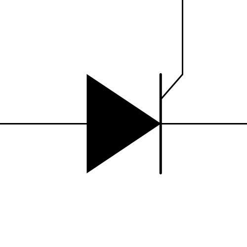 |
|
|
|
|
| Definition: Three pin device with an anode, cathode and the gate, which allows current to flow throughout the thyristor, by application of a small voltage on the gate pin. Used within various fields of DC motor control, generator field regulation, lighting system control and variable frequency drives. |
| Definition: Three pin device with an anode, cathode and the gate, which allows current to flow throughout the thyristor, by application of a small voltage on the gate pin. Used within various fields of DC motor control, generator field regulation, lighting system control and variable frequency drives. |
| Definition: Three pin device with an anode, cathode and the gate, which allows current to flow throughout the thyristor, by application of a small voltage on the gate pin. Used within various fields of DC motor control, generator field regulation, lighting system control and variable frequency drives. |
| Definition: Three pin device with an anode, cathode and the gate, which allows current to flow throughout the thyristor, by application of a small voltage on the gate pin. Used within various fields of DC motor control, generator field regulation, lighting system control and variable frequency drives. |
| Definition: Three pin device with an anode, cathode and the gate, which allows current to flow throughout the thyristor, by application of a small voltage on the gate pin. Used within various fields of DC motor control, generator field regulation, lighting system control and variable frequency drives. |
| Invented in 1957 by William (Bill) Gutzwiller & Gordon Hall. |
| Invented in 1957 by William (Bill) Gutzwiller & Gordon Hall. |
| Invented in 1957 by William (Bill) Gutzwiller & Gordon Hall. |
| Invented in 1957 by William (Bill) Gutzwiller & Gordon Hall. |
| Invented in 1957 by William (Bill) Gutzwiller & Gordon Hall. |
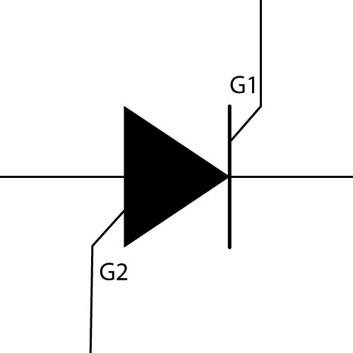 |
|
|
|
|
| Definition: The Silicon Controlled Switch (SCS), is an SCR with an extra gate terminal. The typical load current is carried by the anode gate and cathode terminals, with the cathode gate and anode terminals sufficing as control leads. The SCS is turned on by applying a positive voltage between the cathode gate and cathode terminals and may be turned off by applying a negative voltage between the anode and cathode terminals, or by shorting those two terminals together. The anode terminal must be kept positive to the cathode for the SCS to maintain a latch. |
| Definition: The Silicon Controlled Switch (SCS), is an SCR with an extra gate terminal. The typical load current is carried by the anode gate and cathode terminals, with the cathode gate and anode terminals sufficing as control leads. The SCS is turned on by applying a positive voltage between the cathode gate and cathode terminals and may be turned off by applying a negative voltage between the anode and cathode terminals, or by shorting those two terminals together. The anode terminal must be kept positive to the cathode for the SCS to maintain a latch. |
| Definition: The Silicon Controlled Switch (SCS), is an SCR with an extra gate terminal. The typical load current is carried by the anode gate and cathode terminals, with the cathode gate and anode terminals sufficing as control leads. The SCS is turned on by applying a positive voltage between the cathode gate and cathode terminals and may be turned off by applying a negative voltage between the anode and cathode terminals, or by shorting those two terminals together. The anode terminal must be kept positive to the cathode for the SCS to maintain a latch. |
| Definition: The Silicon Controlled Switch (SCS), is an SCR with an extra gate terminal. The typical load current is carried by the anode gate and cathode terminals, with the cathode gate and anode terminals sufficing as control leads. The SCS is turned on by applying a positive voltage between the cathode gate and cathode terminals and may be turned off by applying a negative voltage between the anode and cathode terminals, or by shorting those two terminals together. The anode terminal must be kept positive to the cathode for the SCS to maintain a latch. |
| Definition: The Silicon Controlled Switch (SCS), is an SCR with an extra gate terminal. The typical load current is carried by the anode gate and cathode terminals, with the cathode gate and anode terminals sufficing as control leads. The SCS is turned on by applying a positive voltage between the cathode gate and cathode terminals and may be turned off by applying a negative voltage between the anode and cathode terminals, or by shorting those two terminals together. The anode terminal must be kept positive to the cathode for the SCS to maintain a latch. |
| Invented in 1967 by Walter R Spofford. |
| Invented in 1967 by Walter R Spofford. |
| Invented in 1967 by Walter R Spofford. |
| Invented in 1967 by Walter R Spofford. |
| Invented in 1967 by Walter R Spofford. |
 |
|
|
|
|
| Definition: The Silicon Unilateral Switch (SUS), is a four-layer diode breakover device, which will breakover in one direction only and is referred to as a unilateral or unidirectional breakover device. They are principally utilised in SCR triggering, however, with addition circuitry, the triac can benefit from this style of trigger. Silicon Unilateral Switches are one of the important unilateral breakover devices as the gate terminal can change its breakover characteristic by connecting a Zener diode between the gate and the cathode (Zener Cathode to SUS Gate & Zener Anode to SUS Cathode). Breakover voltages can be reduced to (VZ + 0.6 V). Reverse breakdown is destructive for the device. |
| Definition: The Silicon Unilateral Switch (SUS), is a four-layer diode breakover device, which will breakover in one direction only and is referred to as a unilateral or unidirectional breakover device. They are principally utilised in SCR triggering, however, with addition circuitry, the triac can benefit from this style of trigger. Silicon Unilateral Switches are one of the important unilateral breakover devices as the gate terminal can change its breakover characteristic by connecting a Zener diode between the gate and the cathode (Zener Cathode to SUS Gate & Zener Anode to SUS Cathode). Breakover voltages can be reduced to (VZ + 0.6 V). Reverse breakdown is destructive for the device. |
| Definition: The Silicon Unilateral Switch (SUS), is a four-layer diode breakover device, which will breakover in one direction only and is referred to as a unilateral or unidirectional breakover device. They are principally utilised in SCR triggering, however, with addition circuitry, the triac can benefit from this style of trigger. Silicon Unilateral Switches are one of the important unilateral breakover devices as the gate terminal can change its breakover characteristic by connecting a Zener diode between the gate and the cathode (Zener Cathode to SUS Gate & Zener Anode to SUS Cathode). Breakover voltages can be reduced to (VZ + 0.6 V). Reverse breakdown is destructive for the device. |
| Definition: The Silicon Unilateral Switch (SUS), is a four-layer diode breakover device, which will breakover in one direction only and is referred to as a unilateral or unidirectional breakover device. They are principally utilised in SCR triggering, however, with addition circuitry, the triac can benefit from this style of trigger. Silicon Unilateral Switches are one of the important unilateral breakover devices as the gate terminal can change its breakover characteristic by connecting a Zener diode between the gate and the cathode (Zener Cathode to SUS Gate & Zener Anode to SUS Cathode). Breakover voltages can be reduced to (VZ + 0.6 V). Reverse breakdown is destructive for the device. |
| Definition: The Silicon Unilateral Switch (SUS), is a four-layer diode breakover device, which will breakover in one direction only and is referred to as a unilateral or unidirectional breakover device. They are principally utilised in SCR triggering, however, with addition circuitry, the triac can benefit from this style of trigger. Silicon Unilateral Switches are one of the important unilateral breakover devices as the gate terminal can change its breakover characteristic by connecting a Zener diode between the gate and the cathode (Zener Cathode to SUS Gate & Zener Anode to SUS Cathode). Breakover voltages can be reduced to (VZ + 0.6 V). Reverse breakdown is destructive for the device. |
| Invented in 1967 by Walter R Spofford. |
| Invented in 1967 by Walter R Spofford. |
| Invented in 1967 by Walter R Spofford. |
| Invented in 1967 by Walter R Spofford. |
| Invented in 1967 by Walter R Spofford. |
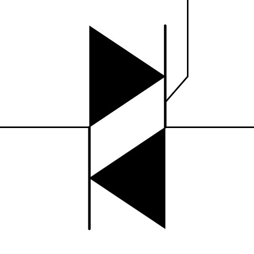 |
|
|
|
|
| Definition: The Triac is a type of thyristor that will conduct current in either direction after the device is placed into a conducting state and will remain there until the voltage-drop across the junction approaches zero. Known as a triode for alternating current, it was formally introduced as the bidirectional triode thyristor or bilateral triode thyristor. The TRIAC has 3 terminals, whereby the Anode or Main Terminal, is depicted as Anode 1, A1 or MT1, Anode 2, A2 or MT2 with G is the Gate. As a subset of thyristors, the triac, is bidirectional (conduct current in both directions), differs from the silicon controlled rectifier (SCR), which is unidirectional (only conducting current in one direction). The gate of the triac can be triggered by either a positive or negative current at their gate, whereas the SCR can only be triggered by a positive current at its gate. When triggered, the triac and the SCR will continue to conduct without gate current and will stop when the main current drops below the holding current. Triacs due to their bidirectional nature, are convenient switches for alternating-current (AC) and in addition, embeds a trigger at a controlled phase angle of the AC waveform to allow for the control of average current flowing into a load (phase control), as with controlling the speed of induction motors, dimming lamps, and controlling electric heaters. |
| Definition: The Triac is a type of thyristor that will conduct current in either direction after the device is placed into a conducting state and will remain there until the voltage-drop across the junction approaches zero. Known as a triode for alternating current, it was formally introduced as the bidirectional triode thyristor or bilateral triode thyristor. The TRIAC has 3 terminals, whereby the Anode or Main Terminal, is depicted as Anode 1, A1 or MT1, Anode 2, A2 or MT2 with G is the Gate. As a subset of thyristors, the triac, is bidirectional (conduct current in both directions), differs from the silicon controlled rectifier (SCR), which is unidirectional (only conducting current in one direction). The gate of the triac can be triggered by either a positive or negative current at their gate, whereas the SCR can only be triggered by a positive current at its gate. When triggered, the triac and the SCR will continue to conduct without gate current and will stop when the main current drops below the holding current. Triacs due to their bidirectional nature, are convenient switches for alternating-current (AC) and in addition, embeds a trigger at a controlled phase angle of the AC waveform to allow for the control of average current flowing into a load (phase control), as with controlling the speed of induction motors, dimming lamps, and controlling electric heaters. |
| Definition: The Triac is a type of thyristor that will conduct current in either direction after the device is placed into a conducting state and will remain there until the voltage-drop across the junction approaches zero. Known as a triode for alternating current, it was formally introduced as the bidirectional triode thyristor or bilateral triode thyristor. The TRIAC has 3 terminals, whereby the Anode or Main Terminal, is depicted as Anode 1, A1 or MT1, Anode 2, A2 or MT2 with G is the Gate. As a subset of thyristors, the triac, is bidirectional (conduct current in both directions), differs from the silicon controlled rectifier (SCR), which is unidirectional (only conducting current in one direction). The gate of the triac can be triggered by either a positive or negative current at their gate, whereas the SCR can only be triggered by a positive current at its gate. When triggered, the triac and the SCR will continue to conduct without gate current and will stop when the main current drops below the holding current. Triacs due to their bidirectional nature, are convenient switches for alternating-current (AC) and in addition, embeds a trigger at a controlled phase angle of the AC waveform to allow for the control of average current flowing into a load (phase control), as with controlling the speed of induction motors, dimming lamps, and controlling electric heaters. |
| Definition: The Triac is a type of thyristor that will conduct current in either direction after the device is placed into a conducting state and will remain there until the voltage-drop across the junction approaches zero. Known as a triode for alternating current, it was formally introduced as the bidirectional triode thyristor or bilateral triode thyristor. The TRIAC has 3 terminals, whereby the Anode or Main Terminal, is depicted as Anode 1, A1 or MT1, Anode 2, A2 or MT2 with G is the Gate. As a subset of thyristors, the triac, is bidirectional (conduct current in both directions), differs from the silicon controlled rectifier (SCR), which is unidirectional (only conducting current in one direction). The gate of the triac can be triggered by either a positive or negative current at their gate, whereas the SCR can only be triggered by a positive current at its gate. When triggered, the triac and the SCR will continue to conduct without gate current and will stop when the main current drops below the holding current. Triacs due to their bidirectional nature, are convenient switches for alternating-current (AC) and in addition, embeds a trigger at a controlled phase angle of the AC waveform to allow for the control of average current flowing into a load (phase control), as with controlling the speed of induction motors, dimming lamps, and controlling electric heaters. |
| Definition: The Triac is a type of thyristor that will conduct current in either direction after the device is placed into a conducting state and will remain there until the voltage-drop across the junction approaches zero. Known as a triode for alternating current, it was formally introduced as the bidirectional triode thyristor or bilateral triode thyristor. The TRIAC has 3 terminals, whereby the Anode or Main Terminal, is depicted as Anode 1, A1 or MT1, Anode 2, A2 or MT2 with G is the Gate. As a subset of thyristors, the triac, is bidirectional (conduct current in both directions), differs from the silicon controlled rectifier (SCR), which is unidirectional (only conducting current in one direction). The gate of the triac can be triggered by either a positive or negative current at their gate, whereas the SCR can only be triggered by a positive current at its gate. When triggered, the triac and the SCR will continue to conduct without gate current and will stop when the main current drops below the holding current. Triacs due to their bidirectional nature, are convenient switches for alternating-current (AC) and in addition, embeds a trigger at a controlled phase angle of the AC waveform to allow for the control of average current flowing into a load (phase control), as with controlling the speed of induction motors, dimming lamps, and controlling electric heaters. |
| Invented in 1957 by William (Bill) Gutzwiller. |
| Invented in 1957 by William (Bill) Gutzwiller. |
| Invented in 1957 by William (Bill) Gutzwiller. |
| Invented in 1957 by William (Bill) Gutzwiller. |
| Invented in 1957 by William (Bill) Gutzwiller. |
| DIODES · TRANSISTORS INTEGRATED CIRCUITS · THYRISTORS THERMIONIC VALVES |
| DIODES · TRANSISTORS INTEGRATED CIRCUITS · THYRISTORS THERMIONIC VALVES |
| DIODES · TRANSISTORS INTEGRATED CIRCUITS · THYRISTORS THERMIONIC VALVES |
| DIODES · TRANSISTORS INTEGRATED CIRCUITS · THYRISTORS THERMIONIC VALVES |
| DIODES · TRANSISTORS INTEGRATED CIRCUITS · THYRISTORS THERMIONIC VALVES |
| Thermionic Valves, an overview |
| Thermionic Valves, an overview |
| Thermionic Valves, an overview |
| Thermionic Valves, an overview |
| Thermionic Valves, an overview |
 |
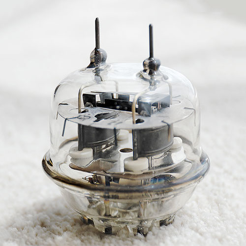 |
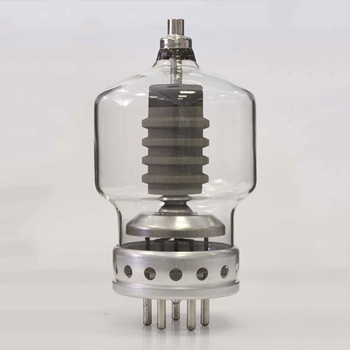 |
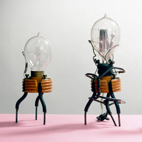 |
|
|
|
|
|
|
|
|
|
|
|
|
|
|
|
|
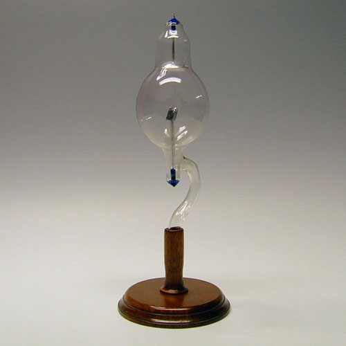 |
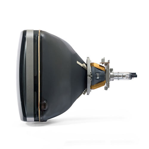 |
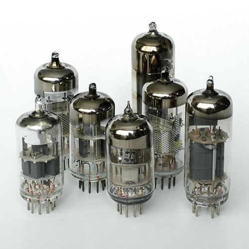 |
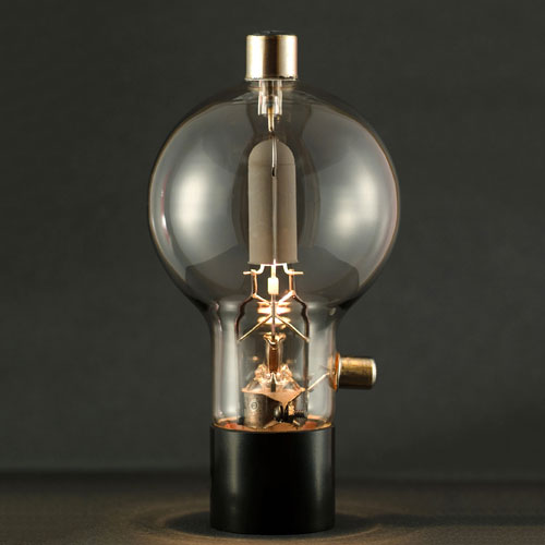 |
|
|
|
|
|
|
|
|
|
|
|
|
|
|
|
|
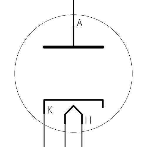 |
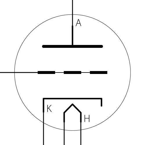 |
 |
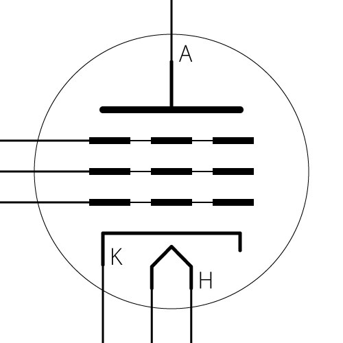 |
||
| Diode | Triode | Tetrode | Pentode |
|
|
|
|
||
| Diode | Triode | Tetrode | Pentode |
|
|
|
|
||
| Diode | Triode | Tetrode | Pentode |
|
|
|
|
||
| Diode | Triode | Tetrode | Pentode |
|
|
|
|
||
| Diode | Triode | Tetrode | Pentode |
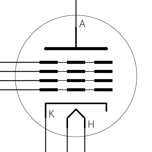 |
 |
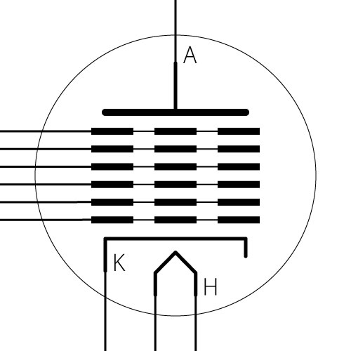 |
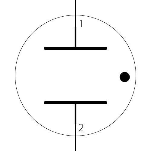 |
||
| Hexode | Heptode | Octode | Gas Discharge |
|
|
|
|
||
| Hexode | Heptode | Octode | Gas Discharge |
|
|
|
|
||
| Hexode | Heptode | Octode | Gas Discharge |
|
|
|
|
||
| Hexode | Heptode | Octode | Gas Discharge |
|
|
|
|
||
| Hexode | Heptode | Octode | Gas Discharge |
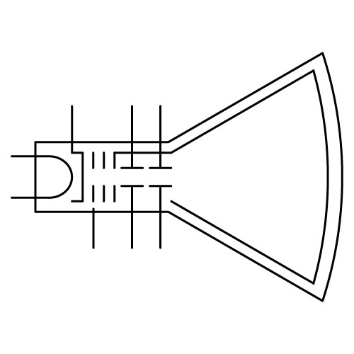 |
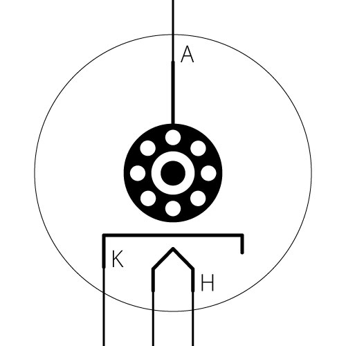 |
||||
| CRT | Magnetron |
|
|
||||
| CRT | Magnetron |
|
|
||||
| CRT | Magnetron |
|
|
||||
| CRT | Magnetron |
|
|
||||
| CRT | Magnetron |
| Includes: Diode, Triode, Tetrode, Pentode, Hexode, Heptode, Octode, Gas Discharge, Cathode Ray (CRT), Magnetron, Carcinotron, Klystron, Photomultiplier, Phototube, Traveling-Wave, Vacuum Fluorescent Display, and X-ray. Definition: Valves rely on thermionic emission of electrons from a cathode filament that is heated by an element and controlled by applying voltage to a grid assembly. Principal uses are for signal amplification, rectification, switching, memory, oscillation and display. |
| Includes: Diode, Triode, Tetrode, Pentode, Hexode, Heptode, Octode, Gas Discharge, Cathode Ray (CRT), Magnetron, Carcinotron, Klystron, Photomultiplier, Phototube, Traveling-Wave, Vacuum Fluorescent Display, and X-ray. Definition: Valves rely on thermionic emission of electrons from a cathode filament that is heated by an element and controlled by applying voltage to a grid assembly. Principal uses are for signal amplification, rectification, switching, memory, oscillation and display. |
| Includes: Diode, Triode, Tetrode, Pentode, Hexode, Heptode, Octode, Gas Discharge, Cathode Ray (CRT), Magnetron, Carcinotron, Klystron, Photomultiplier, Phototube, Traveling-Wave, Vacuum Fluorescent Display, and X-ray. Definition: Valves rely on thermionic emission of electrons from a cathode filament that is heated by an element and controlled by applying voltage to a grid assembly. Principal uses are for signal amplification, rectification, switching, memory, oscillation and display. |
| Includes: Diode, Triode, Tetrode, Pentode, Hexode, Heptode, Octode, Gas Discharge, Cathode Ray (CRT), Magnetron, Carcinotron, Klystron, Photomultiplier, Phototube, Traveling-Wave, Vacuum Fluorescent Display, and X-ray. Definition: Valves rely on thermionic emission of electrons from a cathode filament that is heated by an element and controlled by applying voltage to a grid assembly. Principal uses are for signal amplification, rectification, switching, memory, oscillation and display. |
| Includes: Diode, Triode, Tetrode, Pentode, Hexode, Heptode, Octode, Gas Discharge, Cathode Ray (CRT), Magnetron, Carcinotron, Klystron, Photomultiplier, Phototube, Traveling-Wave, Vacuum Fluorescent Display, and X-ray. Definition: Valves rely on thermionic emission of electrons from a cathode filament that is heated by an element and controlled by applying voltage to a grid assembly. Principal uses are for signal amplification, rectification, switching, memory, oscillation and display. |
| Invented in 1904 by John Ambrose Fleming. |
| Invented in 1904 by John Ambrose Fleming. |
| Invented in 1904 by John Ambrose Fleming. |
| Invented in 1904 by John Ambrose Fleming. |
| Invented in 1904 by John Ambrose Fleming. |
| DIODES · TRANSISTORS INTEGRATED CIRCUITS · THYRISTORS THERMIONIC VALVES · IDENTITY |
| DIODES · TRANSISTORS INTEGRATED CIRCUITS · THYRISTORS THERMIONIC VALVES · IDENTITY |
| DIODES · TRANSISTORS INTEGRATED CIRCUITS · THYRISTORS THERMIONIC VALVES · IDENTITY |
| DIODES · TRANSISTORS INTEGRATED CIRCUITS · THYRISTORS THERMIONIC VALVES · IDENTITY |
| DIODES · TRANSISTORS INTEGRATED CIRCUITS · THYRISTORS THERMIONIC VALVES · IDENTITY |
| Joint Electron Devices Engineering Council Naming Convention for Semiconductors originating in the USA. 1N4001 (Rectifier Diode), 2N2222A (NPN Bipolar Junction Transistor) & 3N143 (Dual Gate FET). Semiconductors can be identified by joining, prefix A, B, number ID, C, suffix D & E, forming the product identification number. SYNTAX: Product ID = A (Prefix) + B (Prefix) + C (Number ID) + D (Suffix) + E (Suffix). A, the first prefix, is established by applying “n – 1”, where “n” is the number of essential connections to the component, less 1. A transistor with 3 essential connections, will result in the use of “2”, as the first prefix. B, the second prefix, is denoted by the component die version, with the letter “C”, or the packaged legacy version of the letter “N”. C, the Number ID, is issued by the JEDEC council and will be greater than 21 for each component class. D, suffix is used for mark sequential revisions with a progressive choice of 10 letters, A, B, C, D, E, F, G, H, J, & K. The letter R, may be used to indicate a reverse-polarity diode in an asymmetrical package, that is mechanically and electrically identical to a forward-polarity device. E, Suffix is reserved for matched pairs of reverse-polarity microwave diodes, using the letters, R & M. |
| Joint Electron Devices Engineering Council Naming Convention for Semiconductors originating in the USA. 1N4001 (Rectifier Diode), 2N2222A (NPN Bipolar Junction Transistor) & 3N143 (Dual Gate FET). Semiconductors can be identified by joining, prefix A, B, number ID, C, suffix D & E, forming the product identification number. SYNTAX: Product ID = A (Prefix) + B (Prefix) + C (Number ID) + D (Suffix) + E (Suffix). A, the first prefix, is established by applying “n – 1”, where “n” is the number of essential connections to the component, less 1. A transistor with 3 essential connections, will result in the use of “2”, as the first prefix. B, the second prefix, is denoted by the component die version, with the letter “C”, or the packaged legacy version of the letter “N”. C, the Number ID, is issued by the JEDEC council and will be greater than 21 for each component class. D, suffix is used for mark sequential revisions with a progressive choice of 10 letters, A, B, C, D, E, F, G, H, J, & K. The letter R, may be used to indicate a reverse-polarity diode in an asymmetrical package, that is mechanically and electrically identical to a forward-polarity device. E, Suffix is reserved for matched pairs of reverse-polarity microwave diodes, using the letters, R & M. |
| Joint Electron Devices Engineering Council Naming Convention for Semiconductors originating in the USA. 1N4001 (Rectifier Diode), 2N2222A (NPN Bipolar Junction Transistor) & 3N143 (Dual Gate FET). Semiconductors can be identified by joining, prefix A, B, number ID, C, suffix D & E, forming the product identification number. SYNTAX: Product ID = A (Prefix) + B (Prefix) + C (Number ID) + D (Suffix) + E (Suffix). A, the first prefix, is established by applying “n – 1”, where “n” is the number of essential connections to the component, less 1. A transistor with 3 essential connections, will result in the use of “2”, as the first prefix. B, the second prefix, is denoted by the component die version, with the letter “C”, or the packaged legacy version of the letter “N”. C, the Number ID, is issued by the JEDEC council and will be greater than 21 for each component class. D, suffix is used for mark sequential revisions with a progressive choice of 10 letters, A, B, C, D, E, F, G, H, J, & K. The letter R, may be used to indicate a reverse-polarity diode in an asymmetrical package, that is mechanically and electrically identical to a forward-polarity device. E, Suffix is reserved for matched pairs of reverse-polarity microwave diodes, using the letters, R & M. |
| Joint Electron Devices Engineering Council Naming Convention for Semiconductors originating in the USA. 1N4001 (Rectifier Diode), 2N2222A (NPN Bipolar Junction Transistor) & 3N143 (Dual Gate FET). Semiconductors can be identified by joining, prefix A, B, number ID, C, suffix D & E, forming the product identification number. SYNTAX: Product ID = A (Prefix) + B (Prefix) + C (Number ID) + D (Suffix) + E (Suffix). A, the first prefix, is established by applying “n – 1”, where “n” is the number of essential connections to the component, less 1. A transistor with 3 essential connections, will result in the use of “2”, as the first prefix. B, the second prefix, is denoted by the component die version, with the letter “C”, or the packaged legacy version of the letter “N”. C, the Number ID, is issued by the JEDEC council and will be greater than 21 for each component class. D, suffix is used for mark sequential revisions with a progressive choice of 10 letters, A, B, C, D, E, F, G, H, J, & K. The letter R, may be used to indicate a reverse-polarity diode in an asymmetrical package, that is mechanically and electrically identical to a forward-polarity device. E, Suffix is reserved for matched pairs of reverse-polarity microwave diodes, using the letters, R & M. |
| Joint Electron Devices Engineering Council Naming Convention for Semiconductors originating in the USA. 1N4001 (Rectifier Diode), 2N2222A (NPN Bipolar Junction Transistor) & 3N143 (Dual Gate FET). Semiconductors can be identified by joining, prefix A, B, number ID, C, suffix D & E, forming the product identification number. SYNTAX: Product ID = A (Prefix) + B (Prefix) + C (Number ID) + D (Suffix) + E (Suffix). A, the first prefix, is established by applying “n – 1”, where “n” is the number of essential connections to the component, less 1. A transistor with 3 essential connections, will result in the use of “2”, as the first prefix. B, the second prefix, is denoted by the component die version, with the letter “C”, or the packaged legacy version of the letter “N”. C, the Number ID, is issued by the JEDEC council and will be greater than 21 for each component class. D, suffix is used for mark sequential revisions with a progressive choice of 10 letters, A, B, C, D, E, F, G, H, J, & K. The letter R, may be used to indicate a reverse-polarity diode in an asymmetrical package, that is mechanically and electrically identical to a forward-polarity device. E, Suffix is reserved for matched pairs of reverse-polarity microwave diodes, using the letters, R & M. |
| Pro Electron Coding System Naming Convention for Semiconductors originating in Europe. BC548 (Silicon, Transistor – audio frequency, low), AF116 (Germanium, Transistor – high frequency, low power) and CL100 (Gallium Arsenide, Transistor – high frequency, power). Semiconductors can be identified by joining, prefix A & B, the number ID, C and suffix D, forming the product identification number. SYNTAX: Product ID = A (Prefix) + B (Prefix) + C (Number ID) + D (Suffix). A, the first prefix, is established by matching the component material: |
| A | Germanium or Band Gap of 0.6 to 1.0eV | ||
| B | Silicon or Band Gap of 1.0 to 1.3eV | ||
| C | Gallium Arsenide or Band Gap greater than 1.3eV | ||
| D | Indium Antimonide or Band Gap less than 0.6eV | ||
| E | (Mullard-Philips) Tubes with a 6.3V heater | ||
| F | Integrated Circuits | ||
| P | (Mullard-Philips) Tubes with a 300 mA heater | ||
| R | Cadmium Sulfide Devices without junctions (LDR) | ||
| S | Integrated Circuits – Solitary | ||
| T | Integrated Circuits – Linear | ||
| U | Integrated Circuits – Digital & Analogue |
| B, the second prefix, is established by matching the intended use of the component: |
| A | Diode – low power or signal | ||
| B | Diode – variable capacitance | ||
| C | Transistor – audio frequency, low | ||
| D | Transistor – audio frequency, power | ||
| E | Tunnel diode | ||
| F | Transistor – high frequency, low power | ||
| G | Hybrid devices | ||
| H | Diode – sensitive to magnetism | ||
| K | Hall effect device | ||
| L | Transistor – high frequency, power | ||
| N | Photocoupler | ||
| P | Light detector | ||
| Q | Light emitter | ||
| R | Switching device, low power, e.g. thyristor, diac, unijunction | ||
| S | Transistor – switching low power | ||
| T | Switching device, low power, e.g. thyristor, triac | ||
| U | Transistor – switching, power | ||
| W | Surface acoustic wave device | ||
| X | Diode multiplier | ||
| Y | Diode rectifying | ||
| Z | Diode – voltage reference |
| C, the Number ID, is issued by the European Electronic Component Manufacturers Association (EECA). |
||
| D, Suffix is used to mark A, for low gain, B, for Medium Gain and C, for High Gain. |
| Japanese Industrial Standard Naming Convention for Semiconductors originating in Japan. BC548 (Silicon, Transistor – audio frequency, low), AF116 (Germanium, Transistor – high frequency, low power) and CL100 (Gallium Arsenide, Transistor – high frequency, power). Semiconductors can be identified by joining, prefix A & B, the number ID, C and suffix D, forming the product identification number. SYNTAX: Product ID = A (Prefix) + B (Prefix) + C (Number ID) + D (Suffix). A, the first prefix, is the number of p-n junctions the component has for the first prefix. B, the second prefix, is established by matching the intended use of the component: |
| A | High frequency PNP BJTs | ||
| B | Audio frequency PNP BJTs | ||
| C | High frequency NPN BJTs | ||
| D | Audio frequency NPN BJTs | ||
| E | Diode | ||
| F | Thyristor | ||
| G | Gunn diode | ||
| H | UJT | ||
| J | P-channel FETs (JFETs & MOSFETs) | ||
| K | N-channel FETs (JFETs & MOSFETs) | ||
| M | TRIAC | ||
| Q | LED | ||
| R | Rectifier | ||
| S | Signal diode | ||
| T | Avalanche diode | ||
| V | Varicap | ||
| Z | Zener Diode |
| C, the Number ID, is the number issued by the Japan Electronics and Information Technology Industries Association and its Electronic DEvice REgistration Centre (JEITA-EDEREC) to assign a part number. D, Suffix is used to mark A (Red), for low gain, B (Orange), for Medium Gain and C (Blue), for High Gain. |
| Component Dimensions |
| Component Dimensions |
| Component Dimensions |
| Component Dimensions |
| Component Dimensions |
| Invented in 1904 by John Ambrose Fleming. |
| Invented in 1904 by John Ambrose Fleming. |
| Invented in 1904 by John Ambrose Fleming. |
| Invented in 1904 by John Ambrose Fleming. |
| Invented in 1904 by John Ambrose Fleming. |
| Integrated Circuits |
| Integrated Circuits |
| Integrated Circuits |
| Integrated Circuits |
| Integrated Circuits |
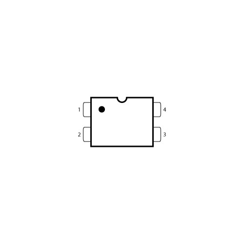
| PDIP 4 |
| PDIP 4 |
| PDIP 4 |
| PDIP 4 |
| PDIP 4 |
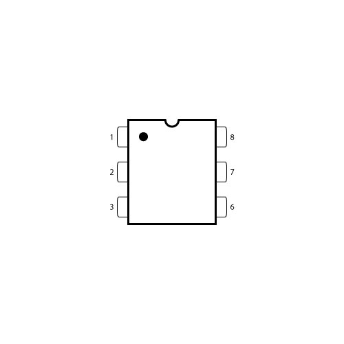
| PDIP 6 |
| PDIP 6 |
| PDIP 6 |
| PDIP 6 |
| PDIP 6 |
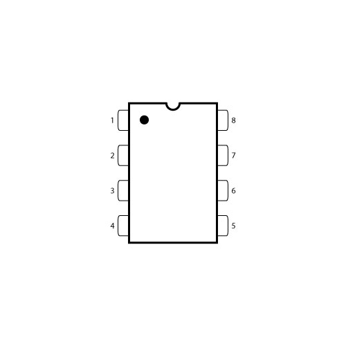
| PDIP 8 |
| PDIP 8 |
| PDIP 8 |
| PDIP 8 |
| PDIP 8 |
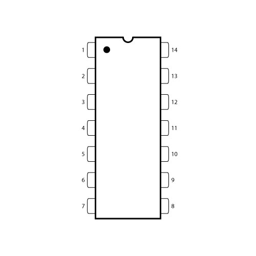
| PDIP 14 |
| PDIP 14 |
| PDIP 14 |
| PDIP 14 |
| PDIP 14 |
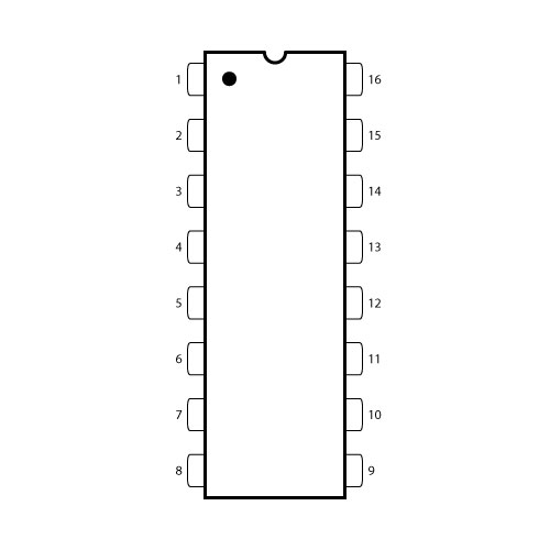
| PDIP 16 |
| PDIP 16 |
| PDIP 16 |
| PDIP 16 |
| PDIP 16 |
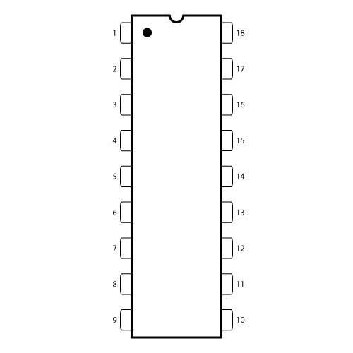
| PDIP 18 |
| PDIP 18 |
| PDIP 18 |
| PDIP 18 |
| PDIP 18 |
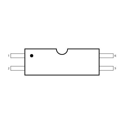
| SODIP 4 |
| SODIP 4 |
| SODIP 4 |
| SODIP 4 |
| SODIP 4 |
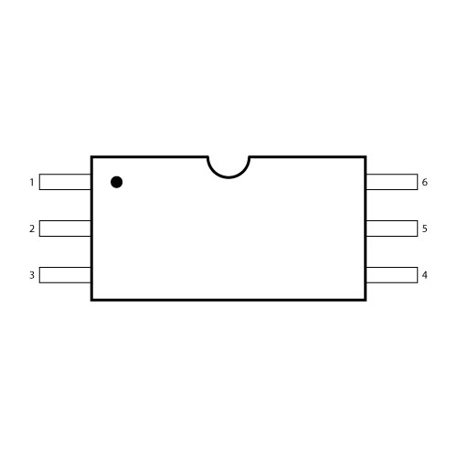
| SODIP 6 |
| SODIP 6 |
| SODIP 6 |
| SODIP 6 |
| SODIP 6 |
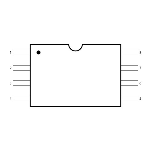
| SODIP 8 |
| SODIP 8 |
| SODIP 8 |
| SODIP 8 |
| SODIP 8 |
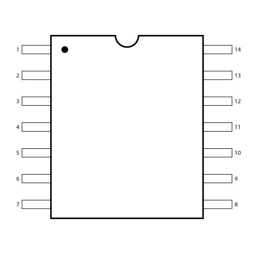
| SODIP 14 |
| SODIP 14 |
| SODIP 14 |
| SODIP 14 |
| SODIP 14 |
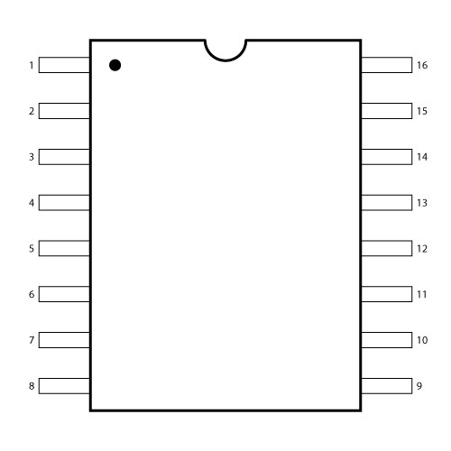
| SODIP 16 |
| SODIP 16 |
| SODIP 16 |
| SODIP 16 |
| SODIP 16 |
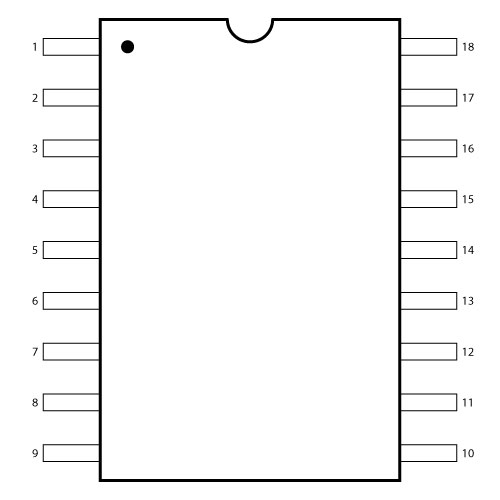
| SODIP 18 |
| SODIP 18 |
| SODIP 18 |
| SODIP 18 |
| SODIP 18 |
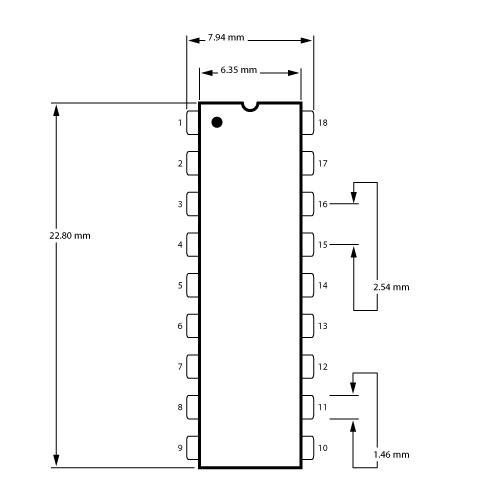
| PDIP Dimensions |
| PDIP Dimensions |
| PDIP Dimensions |
| PDIP Dimensions |
| PDIP Dimensions |
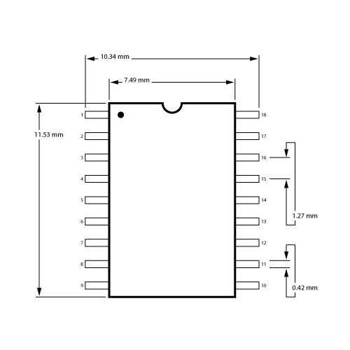
| SODIP Dimensions |
| SODIP Dimensions |
| SODIP Dimensions |
| SODIP Dimensions |
| SODIP Dimensions |