INTELLECTUM VIRTUS
INTELLECTUM VIRTUS
INTELLECTUM VIRTUS
INTELLECTUM VIRTUS
INTELLECTUM VIRTUS
ELECTRICAL ENGINEERING
ELECTRICAL ENGINEERING
ELECTRICAL ENGINEERING
ELECTRICAL ENGINEERING
ELECTRICAL ENGINEERING
DEVELOPMENT
DEVELOPMENT
DEVELOPMENT
DEVELOPMENT
DEVELOPMENT
SCHEMATICS
SCHEMATICS
SCHEMATICS
SCHEMATICS
SCHEMATICS
SCHEMATICS
SCHEMATICS
SCHEMATICS
SCHEMATICS
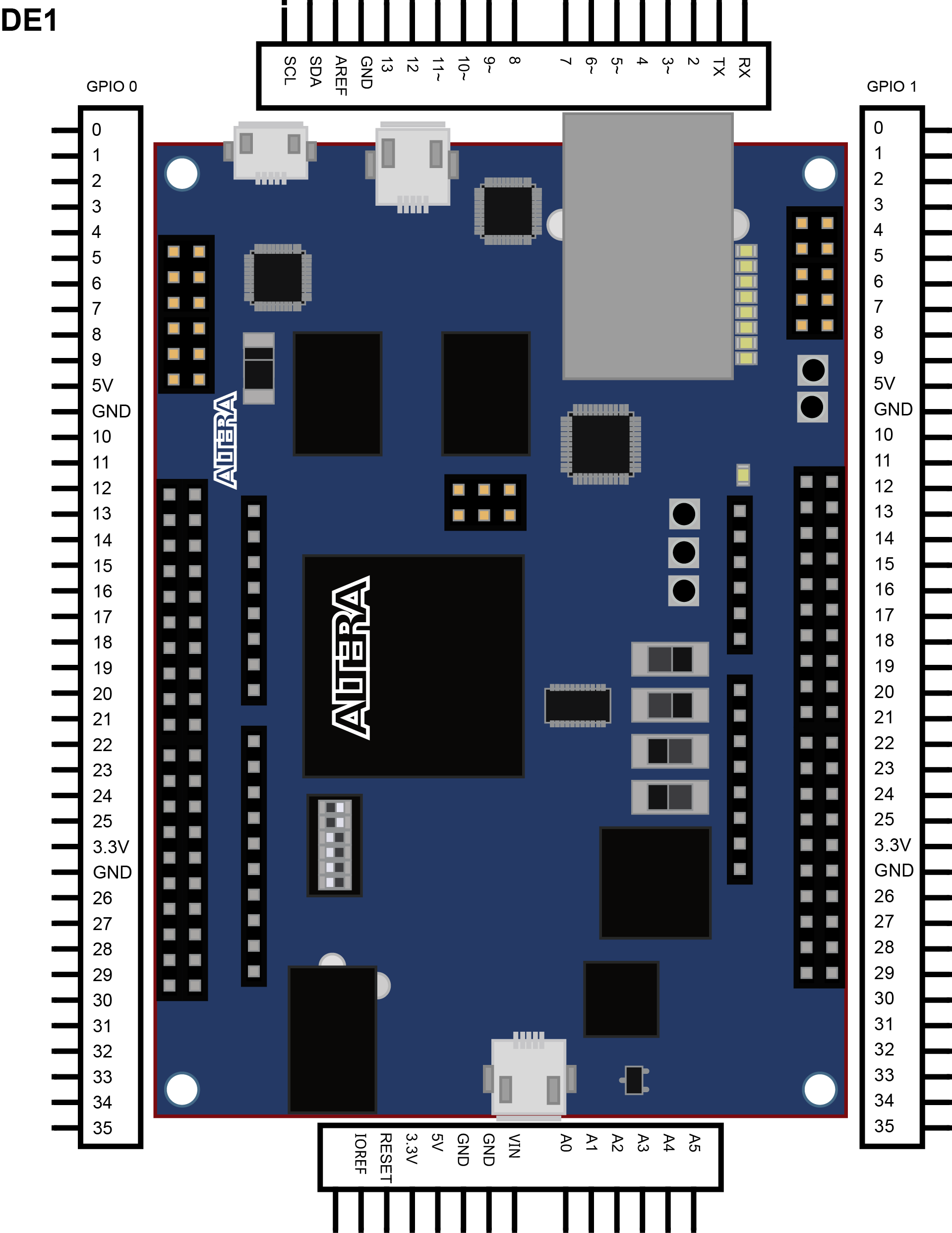
BOARD, DE0 Nano SoC
BOARD, DE0 Nano SoC
BOARD, DE0 Nano SoC
BOARD, DE0 Nano SoC
BOARD, DE0 Nano SoC
In Brief
The DE0-Nano-SoC board is a hardware design platform based on the Altera System-on-Chip (SoC) FPGA, which combines the latest dual-core Cortex-A9 embedded cores with industry-leading programmable logic for ultimate design flexibility. It has many features that allow users to implement a wide range of designed circuits, from simple circuits to various multimedia projects.
FPGA Device
Altera Cyclone® V SE 5CSEMA4U23C6N device; Serial configuration device; USB-Blaster II onboard for programming; JTAG mode; 2 push-buttons; 4 slide-switches; 8 green user LEDs; Three 50MHz clock sources from the clock generator; Two 40-pin expansion header; One Arduino expansion header (Uno R3 compatibility), can connection with Arduino shields; One 10-pin analog input expansion header (shared with Arduino analog input); and A/D converter, 4-pin SPI interface with FPGA.
HPS (Hard Processor System)
925MHz Dual-core ARM Cortex-A9 processor; 1GB DDR3 SDRAM (32-bit data bus); 1 Gigabit Ethernet PHY with RJ45 connector; USB OTG port, USB micro-AB connector; Micro SD card socket; Accelerometer (I2C interface plus interrupt); UART to USB, USB mini-B connector; Warm-reset button and cold-reset button; One user button and one user LED; and LTC 2 x 7 expansion header.
In Detail
The DE0-Nano-SoC Development Kit presents a robust hardware design platform built around the Altera System-on-Chip (SoC) FPGA, which combines the latest dual-core Cortex-A9 embedded cores with industry-leading programmable logic for ultimate design flexibility. Users can now leverage the power of tremendous re-configurability paired with a high-performance, low-power processor system. Altera’s SoC integrates an ARM-based hard processor system (HPS) consisting of processor, peripherals and memory interfaces tied seamlessly with the FPGA fabric using a high-bandwidth interconnect backbone. The DE0-Nano-SoC development board is equipped with high-speed DDR3 memory, analog to digital capabilities, Ethernet networking, and much more that promise many exciting applications.
The DE0-Nano-SoC development kit contains all the tools needed to use the board in conjunction with a computer that runs Microsoft Windows XP or later. This board is designed for the hardware developer. The kit provides reference designs and tutorials to guide you through your first FPGA, HPS, and system designs.
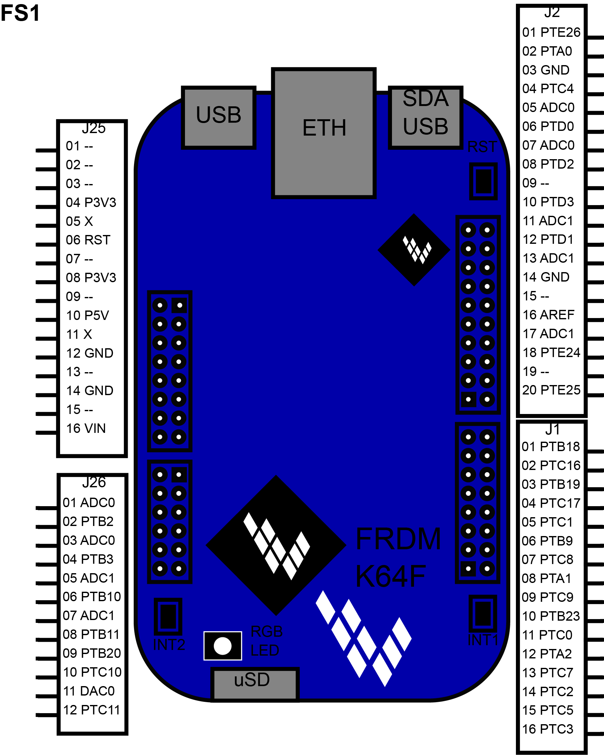
BOARD, Freedom K64F
BOARD, Freedom K64F
BOARD, Freedom K64F
BOARD, Freedom K64F
BOARD, Freedom K64F
In Brief
The Freedom-K64F is an ultra-low-cost development platform for Kinetis K64, K63, and K24 MCUs. It is form-factor compatible with the Arduino R3 pin layout and its peripherals enable rapid prototyping. The board includes a 6-axis digital accelerometer and magnetometer to create full eCompass capabilities, a tri-colored LED and 2 user push-buttons for direct interaction, a microSD card slot, and connectivity using onboard Ethernet port and headers for use with Bluetooth® and 2.4 GHz radio add-on modules. It features OpenSDAv2, the NXP open-source hardware embedded serial and debug adapter running an open-source bootloader.
Features:
MK64FN1M0VLL12 MCU (120 MHz, 1 MB flash memory, 256 KB RAM, low-power, crystal-less USB, and 100 Low profile Quad Flat Package (LQFP))
Dual role USB interface with micro-B USB connector
RGB LED
FXOS8700CQ accelerometer and magnetometer
Two user push buttons
Flexible power supply option – OpenSDAv2 USB, Kinetis K64 USB, and external source
Easy access to MCU input/output through Arduino™ R3 compatible I/O connectors
Programmable OpenSDAv2 debug circuit supporting the CMSIS-DAP Interface software that provides:
Mass storage device (MSD) flash programming interface
CMSIS-DAP debug interface over a driver-less USB HID connection providing run-control debugging and compatibility with IDE tools
Virtual serial port interface
Open source CMSIS-DAP software project
Ethernet
SDHC
Add-on Bluetooth module: JY-MCU BT board V1.05 BT
Software support and application development is offered through the Kinetis software development kit (SDK)
Extensive suite of robust peripheral drivers, stacks and middleware (replacing Sample Code Packages/examples).
In Detail
The NXP Freedom K64 hardware, FRDM-K64F, is a simple, yet sophisticated design featuring a Kinetis K series microcontroller, built on the ARM® Cortex ®-M4 core. FRDM-K64F can be used to evaluate the K64, K63, and K24 Kinetis K series devices. It features the MK64FN1M0VLL12 MCU, which boast the maximum operation frequency of 120MHz, 1MB of flash, 256KB RAM, a full-speed USB controller, Ethernet controller, secure digital host controller, and analog and digital peripherals. The FRDM-K64F hardware is form-factor compatible with the Arduino R3 pin layout, providing a broad range of expansion board options. The onboard interface includes a six-axis digital accelerometer & magnetometer, RGB LED, SDHC, add-on Bluetooth module, add-on RF module, and Ethernet.
The FRDM-K64F platform features OpenSDAv2, the NXP open-source hardware embedded serial and debug adapter running an open-source bootloader. This circuit offers several options for serial communication, flash programming, and run-control debugging. OpenSDAv2 is an mbed™ HDK-compatible debug interface preloaded with the open-source CMSIS-DAP Interface firmware (mbed interface) for rapid prototyping and product development, with a focus on connected Internet of Things devices.
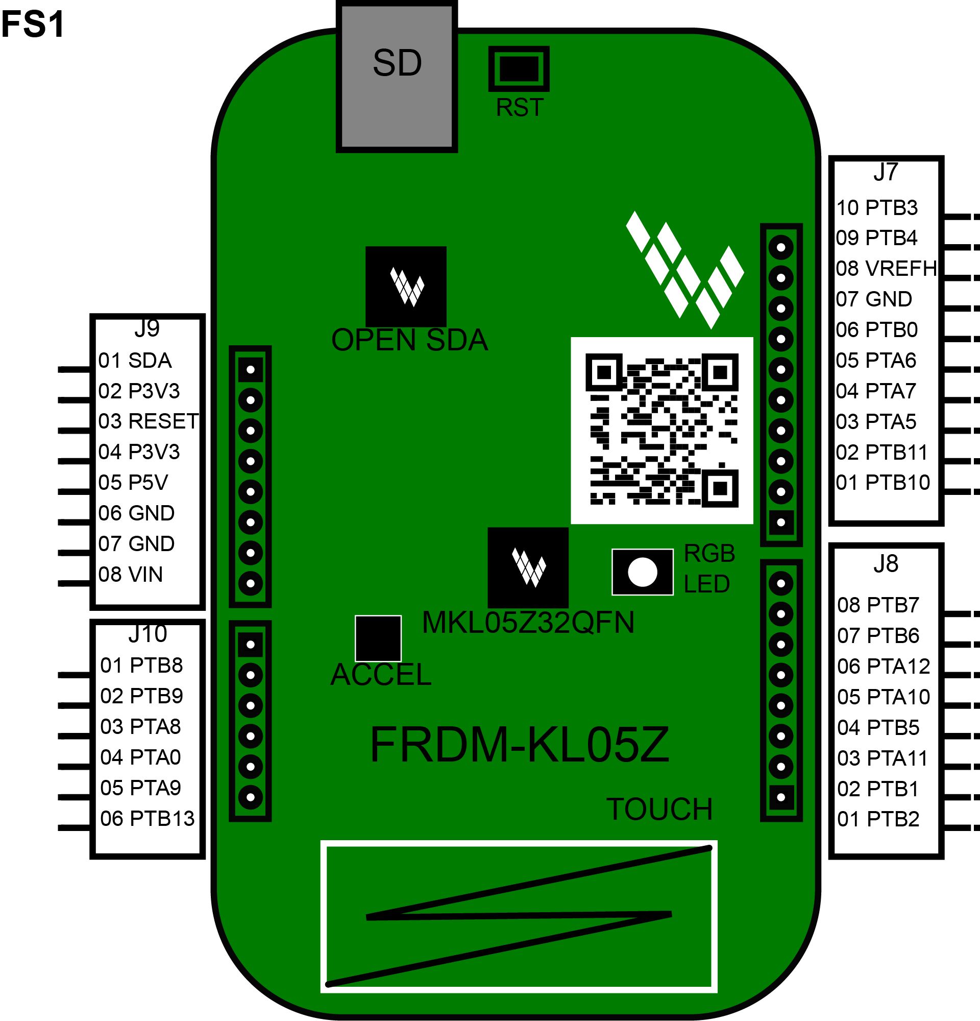
BOARD, Freedom KL05Z
BOARD, Freedom KL05Z
BOARD, Freedom KL05Z
BOARD, Freedom KL05Z
BOARD, Freedom KL05Z
In Brief
The FRDM-KL05Z is an ultra-low-cost development platform enabled by the Kinetis® L Series KL0x MCU family built on the ARM® Cortex®-M0+ processor. Features include easy access to MCU I/O, battery-ready, low-power operation, a standard-based form factor with expansion board options and a built-in debug interface for flash programming and run-control. The FRDM-KL05Z is supported by a range of NXP® and third-party development software.
Features:
MKL05Z32VFM4 MCU – 48 MHz, 32 KB flash, 4 KB SRAM, 32QFN
Capacitive touch slider, MMA8451Q accelerometer, tricolor LED
Easy access to MCU I/O
Sophisticated OpenSDA debug interface
Mass storage device flash programming interface (default) – no tool installation required to evaluate demo apps
P&E Multilink interface provides run-control debugging and compatibility with IDE tools
In Detail
The NXP Freedom KL05Z hardware, FRDM-KL05Z, is a simple, yet sophisticated design featuring a Kinetis L series microcontroller, the industry’s first microcontroller built on the ARM® Cortex™-M0+ core. FRDM-KL05Z can be used to evaluate the KL04 and KL05 Kinetis L series devices. It features a MKL05Z32VFM4, a KL0 family device boasting a max operating frequency of 48MHz, 32KB of flash, and a multitude of analog and digital peripherals.
The FRDM-KL05Z hardware is form-factor compatible with the Arduino™ R3 pin layout, providing a broad range of expansion board options. The on-board interfaces include an RGB LED, a 3-axis digital accelerometer, and a capacitive touch slider. The FRDM-KL05Z also features the open standard embedded serial and debug adapter known as OpenSDA. This circuit offers several options for serial communications, flash programming and run-control debugging.
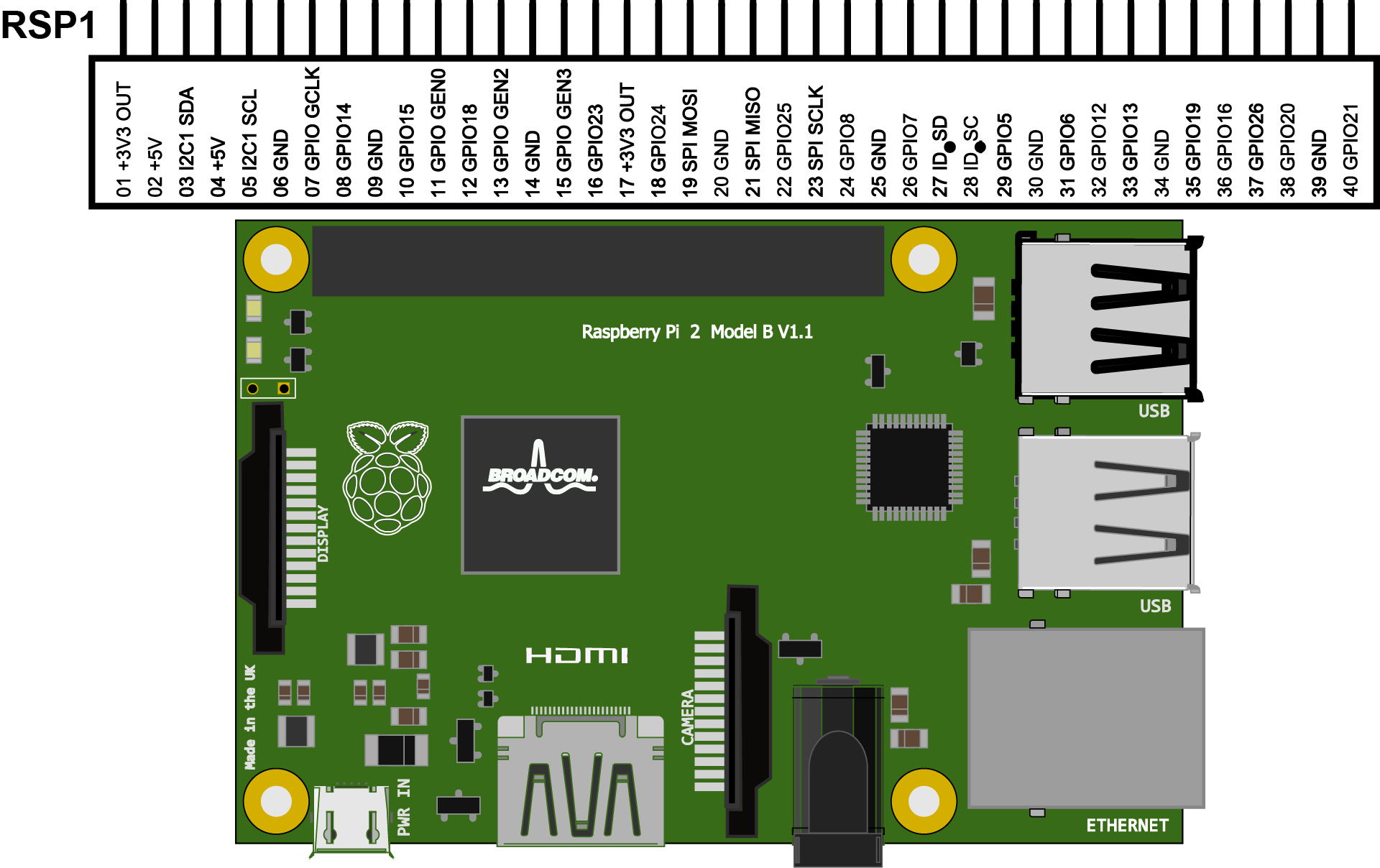
BOARD, Raspberry Pi 2, Model B
BOARD, Raspberry Pi 2, Model B
BOARD, Raspberry Pi 2, Model B
BOARD, Raspberry Pi 2, Model B
BOARD, Raspberry Pi 2, Model B
In Brief
The Raspberry Pi 2 Model B is the second generation Raspberry Pi. It replaced the original Raspberry Pi 1 Model B+ i. Compared to the Raspberry Pi 1 it has:
900MHz quad-core ARM Cortex-A7 CPU
1GB RAM
Like the (Pi 1) Model B+, it also has:
4 USB ports
40 GPIO pins
Full HDMI port
Ethernet port
Combined 3.5mm audio jack and composite video
Camera interface (CSI)
Display interface (DSI)
Micro SD card slot
VideoCore IV 3D graphics core
In Detail
The Raspberry Pi 2 Model B is built around the ARMv7 processor, a 900MHz quad-core ARM Cortex-A7 CPU enabling the Raspberry Pi to run a vast range of ARM GNU/Linux distributions, including Snappy Ubuntu Core, as well as Microsoft Windows 10. The upgrade of processor in this platform, from BCM2835 (single core ARMv6) to BCM2836 (quad core ARMv7), means 2X increase in performance. The board also comes with a full gigabyte of RAM, which will greatly improve games and web-browser performance.
The board is powered through a USB Micro power supply. The power supply requires to provide at least 700mA at 5V. The Raspberry Pi 2 has an identical form factor to the previous (Pi 1) Model B+ and has complete compatibility with Raspberry Pi 1.
BOARD, Raspberry Pi 3, Model B
BOARD, Raspberry Pi 3, Model B
BOARD, Raspberry Pi 3, Model B
BOARD, Raspberry Pi 3, Model B
BOARD, Raspberry Pi 3, Model B
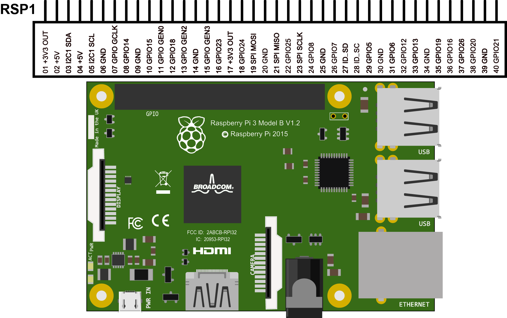
In Brief
The Raspberry Pi 3 is the third generation Raspberry Pi model. It replaces the Raspberry Pi 2 Model B. Compared to the Raspberry Pi 2 it has the following upgrades:
1.2GHz 64-bit quad-core ARMv8 CPU
802.11n Wireless LAN
Bluetooth 4.1
Bluetooth Low Energy (BLE)
1GB RAM
4 USB ports
40 GPIO pins
Full HDMI port
Ethernet port
Combined 3.5mm audio jack and composite video
Camera interface (CSI)
Display interface (DSI)
Micro SD card slot (now push-pull rather than push-push)
VideoCore IV 3D graphics core
In Detail
The Raspberry Pi 3 is powered by a USB Micro power supply (like most standard mobile phone chargers). A good-quality power supply that provide at least 2A at 5V are recommended for the Model 3B, or 700mA at 5V for the earlier, lower powered models. Low current (~700mA) power supplies will work for basic usage, but are likely to cause the Pi to reboot if it draws too much power. Any standard USB keyboard and mouse will work with your Raspberry Pi. For display, any HDMI/DVI monitor and any TV should work as a display for the Pi. For best results, use one with HDMI input, but other connections are available for older devices. For Memory allocation, it is recommended 8GB class 4 SD card. An Ethernet cable is used to connect your Pi to a local network and the internet. Alternatively, users can connect to a wireless network using a USB wireless dongle, which will require configuration.
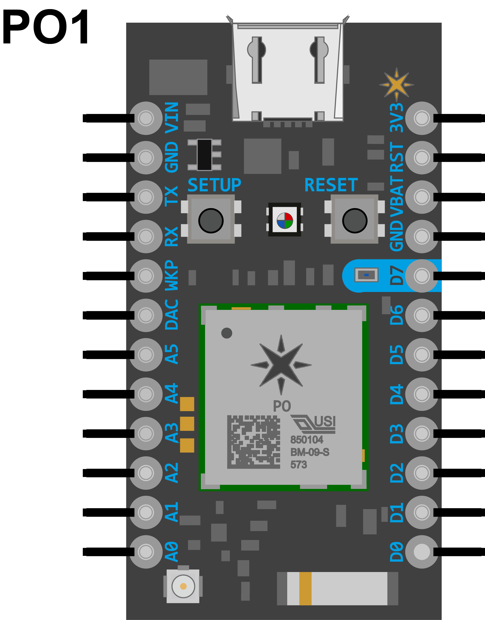
BOARD, WRL 13764 Particle IoT
BOARD, WRL 13764 Particle IoT
BOARD, WRL 13764 Particle IoT
BOARD, WRL 13764 Particle IoT
BOARD, WRL 13764 Particle IoT
In Brief
Particle’s IoT (Internet of Things) hardware development board, the Photon, provides everything needed to build a connected project. Particle has combined a powerful microcontroller with a Wi-Fi chip in a tiny thumbnail-sized module called the PØ (P-Zero):
Particle PØ Wi-Fi module
Broadcom BCM43362 Wi-Fi chip
802.11b/g/n Wi-Fi
STM32F205 120Mhz ARM Cortex M3
1MB flash, 128KB RAM
On-board RGB status LED (ext. drive provided)
18 Mixed-signal GPIO and advanced peripherals
Open source design
Real-time operating system (FreeRTOS)
Soft AP setup
FCC, CE, and IC certified
No Headers Included
In Detail
This Photon board features the PØ WI-FI module, which is a combination of a STM32F205 120Mhz ARM Cortex M3 microcontroller and a Broadcom BCM43362 Wi-Fi chip. These specific Photons come without headers, making them best for surface mounting and special applications. The Photon is not only powerful, but easy to use. The small form factor is ideal for IoT projects with cloud-connectivity. To get started quickly, Particle has added a rock solid 3.3VDC SMPS power supply, RF and user interface components to the PØ all on a small single-sided PCB.
The Photon comes with access to the Particle Cloud, a free cloud service. The Particle Cloud has some great features for building connected projects, including over-the-air firmware updates, an easy-to-use REST API, and firmware development supported by web and local IDEs.