INTELLECTUM VIRTUS
INTELLECTUM VIRTUS
INTELLECTUM VIRTUS
INTELLECTUM VIRTUS
INTELLECTUM VIRTUS
ELECTRICAL ENGINEERING
ELECTRICAL ENGINEERING
ELECTRICAL ENGINEERING
ELECTRICAL ENGINEERING
ELECTRICAL ENGINEERING
COMMUNICATIONS
COMMUNICATIONS
COMMUNICATIONS
COMMUNICATIONS
COMMUNICATIONS
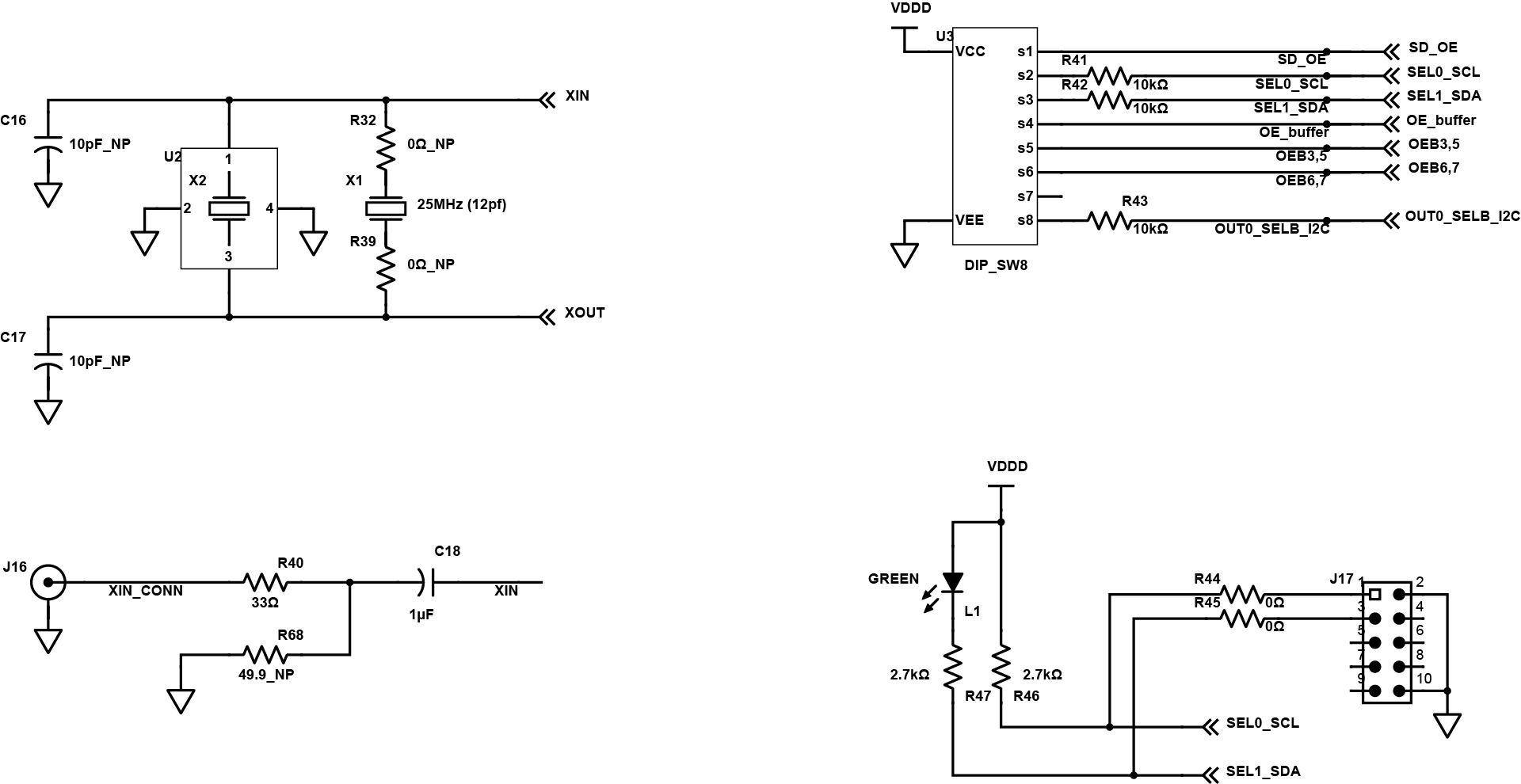
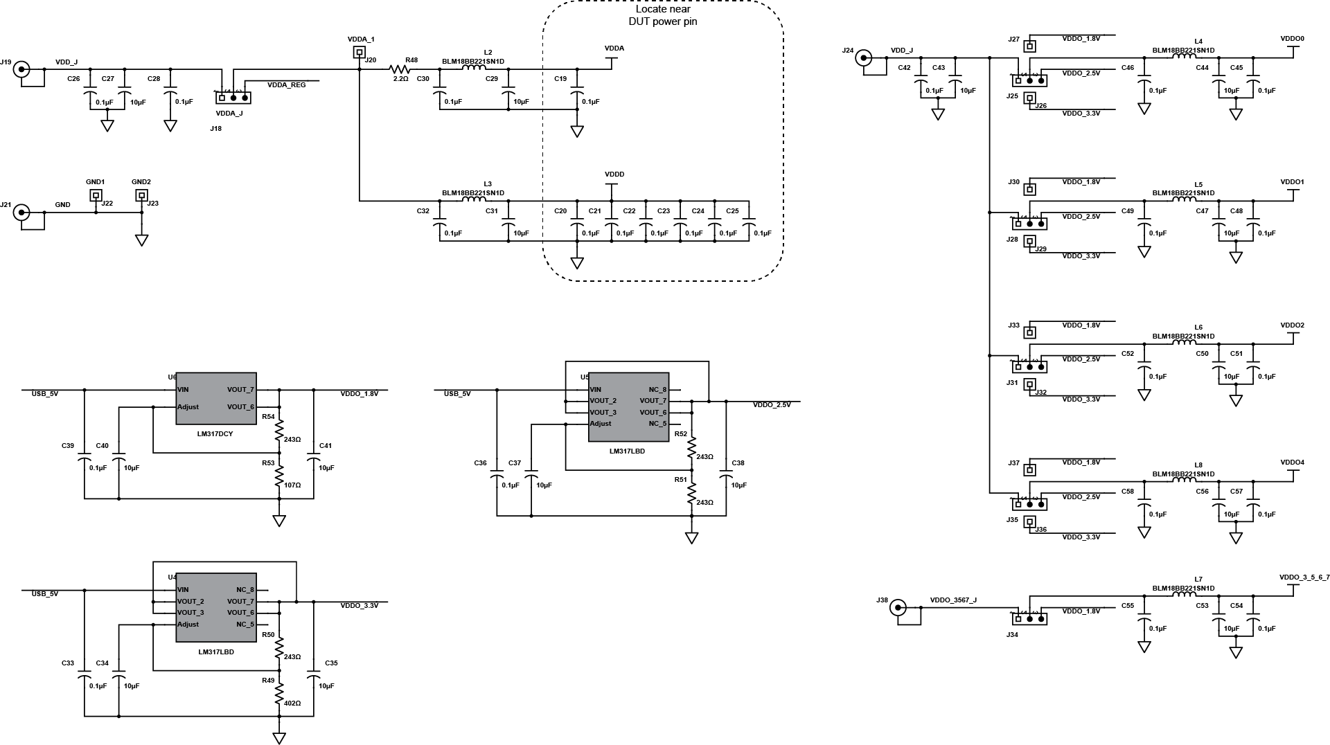
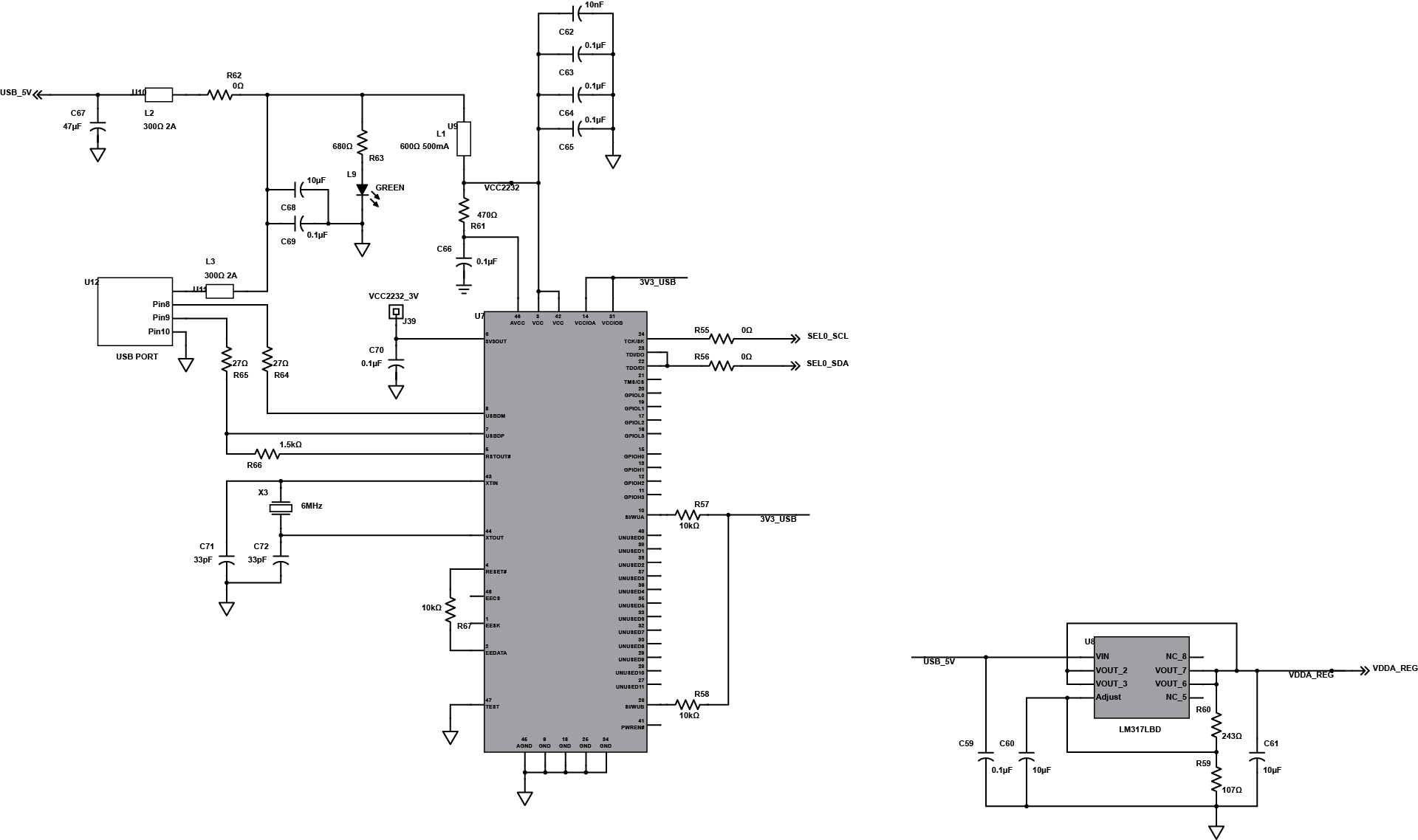
SCHEMATICS
SCHEMATICS
SCHEMATICS
SCHEMATICS
SCHEMATICS
SCHEMATICS
SCHEMATICS
SCHEMATICS
SCHEMATICS
ADAPTER, M.2 NGFF to USB3.0
ADAPTER, M.2 NGFF to USB3.0
ADAPTER, M.2 NGFF to USB3.0
ADAPTER, M.2 NGFF to USB3.0
ADAPTER, M.2 NGFF to USB3.0
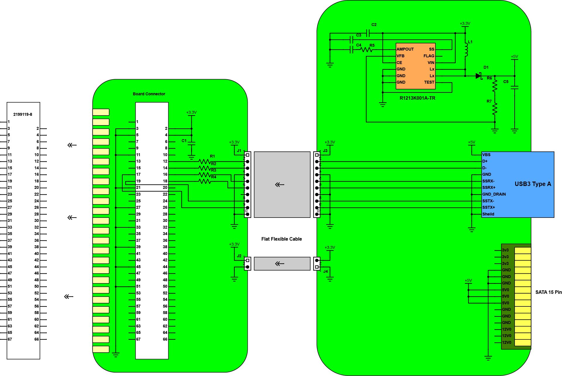
In Brief
The M.2 NGFF to USB3.0 Extend Board is designed with TE Connectivity’s 2199119-8 socket, which allows USB 3.0 device to type 2242 Key B M.2 type slot in the Desktop or Laptop. It supports type 2230 M.2 Card dimension and M.2 key B card type. The standard 15-pin SATA external power requires a 5V supply. This project is designed both single and double-sided modules having a 0.5mm pitch width with 67 positions.
In Detail
The M.2 stands for next generation form factor developed for flat and high-efficiency equipment such as ultrabook or tablet PCs. It is a natural transition from the Mini Card and Half Mini Card to a smaller form factor in both size and volume which supports multiple function add-in cards/modules including: Wi-Fi, Bluetooth, global navigation satellite systems, near field communication, Hybrid digital radio, wireless gigabit alliance (WiGig), wireless wide area network and solid-state storage devices. Also adds functionality to USB 3.0, display Port, SDIO and SSD-PCIe.
The TE connectivity’s (TE) M.2 next-generation form factor (NGFF) connectors, which are designed using the new interface standard for a smaller form factor in both size and volume has various applications that are found in notebooks, ultrabooks & desktops, tablets, servers, portable gaming devices, devices that require SSDs, portable mobile devices. It is engineered for a wide range of applications that meets both current and future market needs for slim solutions. This product line offers a natural progression from the Mini Card and Half Mini Card to a smaller overall form factor making it suitable for thin platform applications. M.2 (NGFF) connectors can save more than 20% PCB real estate compared to PCIe Mini Card, and reduce connector height by 15%.
AMPLIFIER, Telecommunications, RF at 2100MHz
AMPLIFIER, Telecommunications, RF at 2100MHz
AMPLIFIER, Telecommunications, RF at 2100MHz
AMPLIFIER, Telecommunications, RF at 2100MHz
AMPLIFIER, Telecommunications, RF at 2100MHz
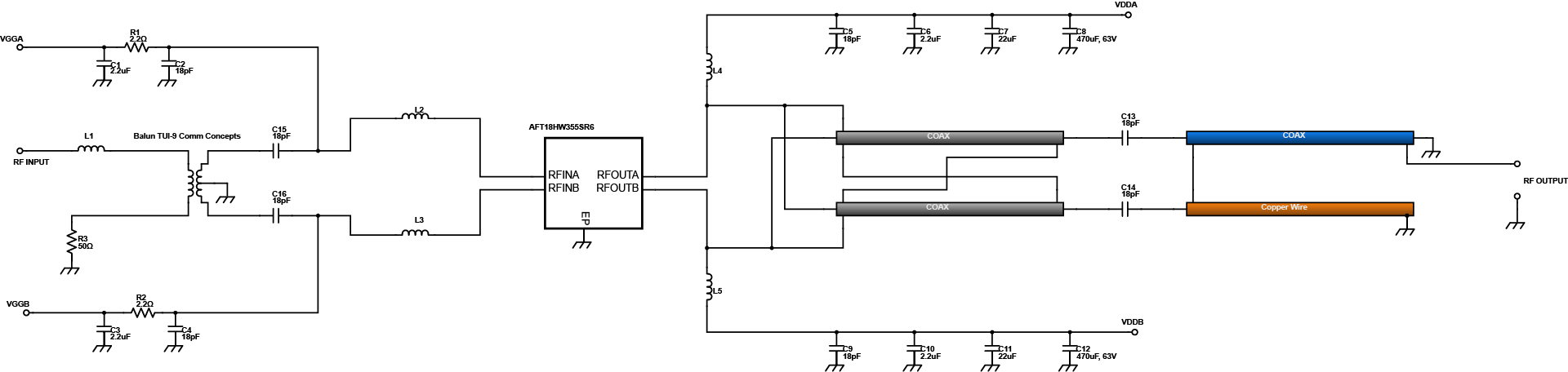
In Brief
Our telecommunication data usage is rapidly increasing in which Internet Service Providers (ISPs) are having difficulties in managing the demand of their customers. This problem is caused by the number of people that are now into digital communications, which smartphones provide them access to the internet anywhere they want as long as there is a GSM signal. This design features an RF Power LDMOS Transistor that is used in 2100MHz RF Power Amplifier. The 2100MHz frequency band is a WCDMA air interface standard, which is also a basis of Universal Mobile Telecommunications System (UMTS). It has digital predistortion error correction system and great negative gate-source voltage range for improved class C operation that are good for cellular base station applications.
In Detail
The design is comprised of AFT18HW355SR6 Airfast RF Power LDMOS Transistor that offers high output power with a corresponding drain to source breakdown voltage. The coaxial cables are used for better efficiency while the copper wire attached to the ground helps in minimizing fluctuation and noise. The coils are used to improve the amplitude of the given frequency, which helps during an increase of attenuation. The TUI-9 RF transformer is for input impedance matching. The RC network is used as filter of the bias voltage.
This design is useful in rural areas where GSM signal is low. It is much cheaper compared to other RF equipment that require a lot of external components. It is also suitable for RF signal development that it can be modified with respect to the application requirements.
AUTOMATION, Home, Zigbee
AUTOMATION, Home, Zigbee
AUTOMATION, Home, Zigbee
AUTOMATION, Home, Zigbee
AUTOMATION, Home, Zigbee
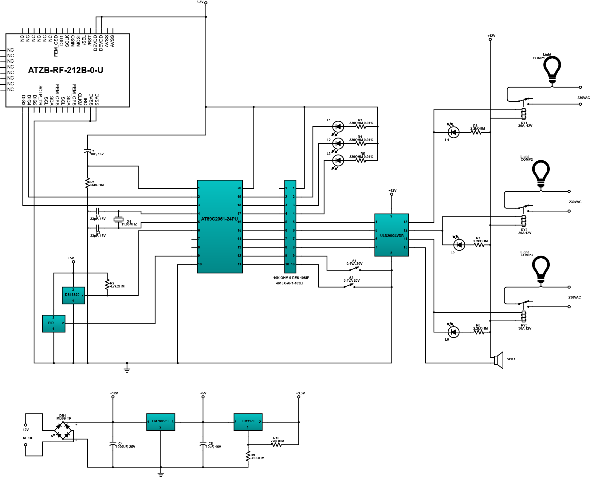
In Brief
This design features a typical application of wireless zigbit module that is home automation. It optimized the system sensors and energy consumptions that provide convenience to users. It is compact in size and easily configured to provide real-time update to the system. It is also mesh networking capable and can be operate license-free worldwide.
In Detail
The design uses ATZB-RF-212B-0-U Zigbit 900MHz wireless module that provide the zigbee communication protocol between the host system and I/O components. The AT89C2051-24PU 8-bit MCU manages the I/O components with the commands uploaded into it. It uses relay driver that supports the low voltage relay for switching the lamp. The system have proximity and temperature sensors that detects human presence and some related objects that need to be considered. The speaker can be used for alarm or delivering a simple signal or message. In the power supply side, it uses two Low DropOut (LDO) regulator to provide 3.3V and 5V while a 12V supply is also provided after diode bridge.
The design can be used in energy saving system of commercial and residential applications. It can be used in industrial application but requires some modifications so that it will fit to the system.
SIGNAL, VersaClock, 5-Clock Generator
SIGNAL, VersaClock, 5-Clock Generator
SIGNAL, VersaClock, 5-Clock Generator
SIGNAL, VersaClock, 5-Clock Generator
SIGNAL, VersaClock, 5-Clock Generator
5P49V5907
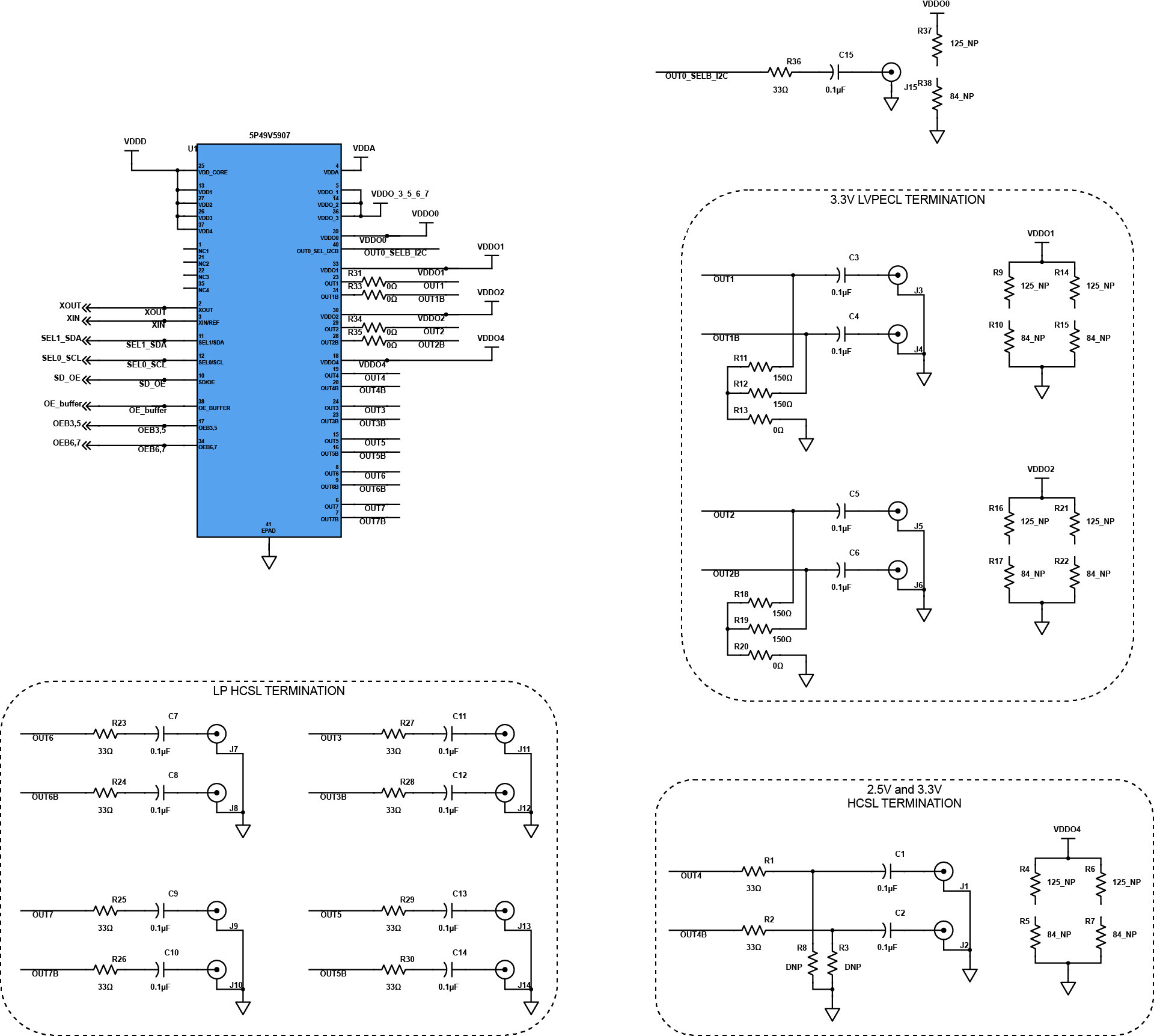
VC5
Power
I2C Module
In Brief
The clock generator produces a timing signal (clock signal) for synchronizing a circuit’s operation. The VersaClock 5 is ideal for high-performance consumer, networking, industrial, computing, and data-communications applications. This circuit design is the evaluation board for the 5P49V5907 programmable clock generator with RMS phase jitter is less than 0.75 picoseconds over the full 12kHz to 20MHz integration range. The device meets the stringent jitter requirements of PCI Express Gen 1/2/3, USB 3.0, and 1G / 10G Ethernet.
In Detail
The circuit design features four copies of Low Power HCSL (LP-HCSL) outputs and three Universal Differential Outputs capable of generating any output frequency using IDT Timing Commander Software. The board is connected to a PC through a USB connector for configuring and programming the device. The USB interface will provide +5V power supply to the board, from which on-board voltage regulators generate various voltages for the core as well as for each output. The board can also be powered by a bench power supply by connecting two banana jacks for output and core voltages, respectively.
The 5P49V5907 clock generator is designed for high performance operation. This is majorly used on networking, industrial, computing, and data communication applications. The configurations can be stored in on-chip One-Time Programmable (OTP) memory and/or can be reconfigured using I2C interface. Also, the frequencies are generated from a single reference clock or crystal.
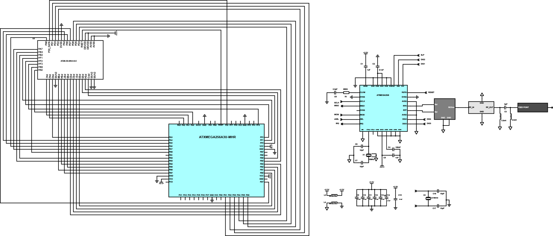
TRANSCEIVER, ZigBit at 2.4GHz
TRANSCEIVER, ZigBit at 2.4GHz
TRANSCEIVER, ZigBit at 2.4GHz
TRANSCEIVER, ZigBit at 2.4GHz
TRANSCEIVER, ZigBit at 2.4GHz
In Brief
This reference design is comprised of Atmel’s promising ATZB-X0-256-3-0-C ZigBit MCU which is an ultra compact, low power and high sensitivity module. Based on a solid combination of the latest Atmel MCU Wireless hardware platform, 2.4GHz ISM band transceiver and Atmel Studio Wireless Composer – the ZigBit offers an unmatched combination of superior radio performance, ultra-low power consumption and exceptional ease of integration.
In Detail
This ZigBit module contains Atmel’s ATxmega256A3U Microcontroller and AT86RF233 2.4GHz ISM band Transceiver for ZigBee and IEEE 802.15.4 [1]. The module features 256KB in-system self-programmable Flash memory, 16KB SRAM and 4KB EEPROM. The compact all-in-one board design of MCU and radio transceiver with very minimal components on the RF path to Antenna dramatically improves the ZigBit’s compact size, range performance on signal transmission and increases its sensitivity. This ensures stable connectivity within a larger coverage area, and helps develop applications on smaller footprint. The MS-147 connector [2] can be used as an RF Test port. ZigBit Module contains a complete RF/MCU design with all the necessary passive components included. The module can be easily mounted on a simple 2-layer PCB with a minimum of required external connection. The ZigBit Module evaluation kit containing the ZigBit extension board for the Atmel Xplained PRO HW evaluation platform can be used to develop FW using the Atmel Studio and evaluate using the Wireless Composer. Compared to a custom RF/MCU solution, a module-based solution offers considerable savings in development time and NRE cost per unit during the HW/FW design, prototyping, and mass production phases of product development. All ZigBits are preloaded with a bootloader when they are sold as modules, either in single units or T&R. Depending on end-user design requirements, the ZigBit can operate as a self-contained sensor node, where it would function as a single MCU, or it can be paired with a host processor driving the module over a serial interface.
The Zigbit module has various applications such as for building automation and monitoring, HVAC monitoring, inventory management, environmental monitoring, security and any other related industrial monitoring.
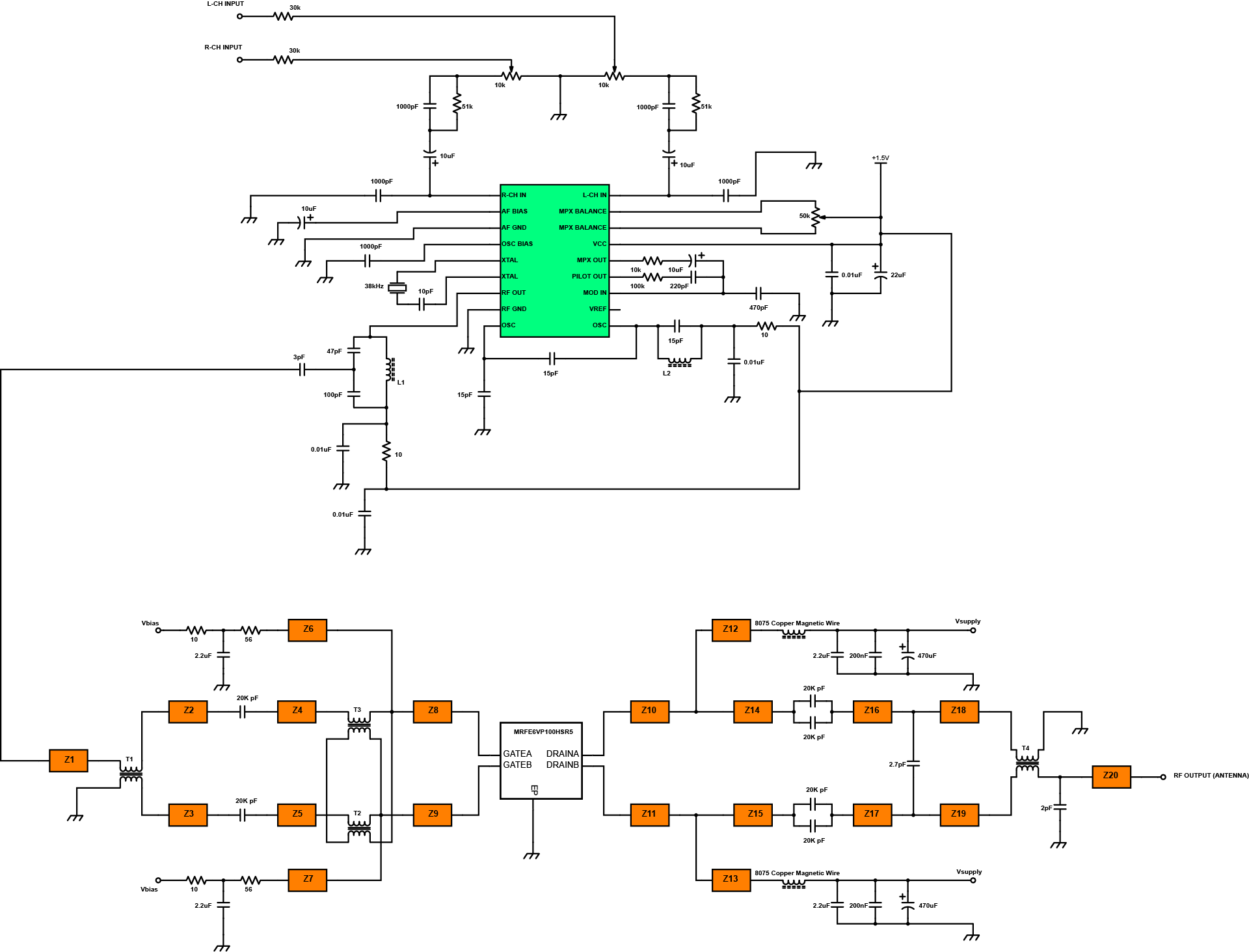
TRANSCEIVER, FM Stereo at 100W
TRANSCEIVER, FM Stereo at 100W
TRANSCEIVER, FM Stereo at 100W
TRANSCEIVER, FM Stereo at 100W
TRANSCEIVER, FM Stereo at 100W
In Brief
Creating a HI-FI stereo FM transmitter to transmit music around the house or even for your own radio station can be sometimes really challenging. Designing preamplifiers, buffers, RF oscillators, modulators, and RF amplifiers add to the difficulty of building an FM transmitter. With this circuit, we can minimize the complexity of creating stereo FM transmitters.
In Detail
This circuit uses a HI-FI Stereo FM Transmitter IC. This IC serves as the low power stage of the transmitter and it can be powered by a 1.25V-2.5V DC supply voltage. It consists of a stereo modulator that creates stereo composite signals, an FM modulator that creates FM signals, and an RF amplifier. The stereo modulator develops composite signals made up of a MAIN (L+R) signal, a SUB (L-R) signal, and a pilot (19kHz) signal using 38kHz crystal oscillator. The FM modulator has carriers on the broadcast band (88-108 MHz). The RF amplifier transmits the stereo encoded FM signals and is also a buffer for the FM modulator.
The MRFE6VP100HSR5 in this circuit serves as its RF Power LDMOS transistors. With the use of some components, the MRFE6VP100HSR5 acts as its power amplifier and amplifies the signal it receives from the stereo FM transmitter IC output. The MRFE6VP100HSR5 circuit is configured as a broadband power amplifier covering frequencies from 30MHz up to 512MHz. It can be supplied by a 50V power supply able to provide at least 100W power. The MRFE6VP100HSR5 can also provide 100W PEP power with a gain of 19.0dB.
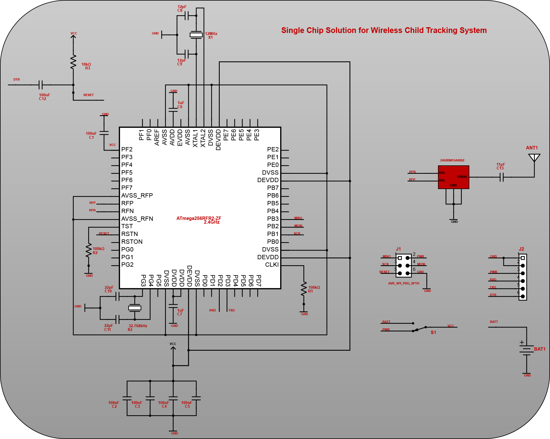
TRANSMITTER, RF Single-Chip Tracker
TRANSMITTER, RF Single-Chip Tracker
TRANSMITTER, RF Single-Chip Tracker
TRANSMITTER, RF Single-Chip Tracker
TRANSMITTER, RF Single-Chip Tracker
In Brief
This system is designed to allow school teachers track children’s interactions using ATmega256RFR2-ZF RF microcontroller. For this design, children are equipped with tags and stations are installed in key locations, which will be able to detect when a child is nearby. Also, a web application will be provided for the parents to remotely monitor the activities of their kid in school.
In Detail
The Atmel ATmega256RFR2 is the leading device in this single-chip family, as well as the most efficient device on the market. With the newest device, the family now has an expanded offering range of 64K to 256K of Flash memory, enabling you to easily scale your designs. With the introduction of the advanced hardware-assisted reduced power consumption (RPC) capability, the ATmega RFR2 family now consumes up to 50 percent less current in some operating modes. It allows for 16 MHz operations at as low as 1.8V of supply voltage and fast wake-up time from sleep mode to active modes. A variety of power-down modes, such as a wake-on-radio feature, which keeps the RF transceiver active while the microcontroller sleeps, further enhance efficiency.
The ATmega256RFR2-ZF microcontroller’s high data rate modes up to 2Mbit/s are available to support general-purpose 2.4GHz ISM applications. A low-power single-chip design lets you implement the latest battery-driven systems, save board space, and reduce bill of materials (BOM) costs.